
Official websites use .gov
A .gov website belongs to an official government organization in the United States.
Secure .gov websites use HTTPS
A lock (
) or https:// means you’ve safely connected to the .gov website. Share sensitive information only on official, secure websites.
Quantitative Nanostructure Characterization Group
The projects within the group are highly interconnected to cover metrology and standards development as well as pursue novel device concepts, particularly for wide band gap semiconductors, magnetic nanomaterials and 2D materials. We maintain active collaborations with other groups at NIST and academic and industrial groups around the world.
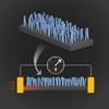
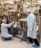
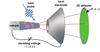
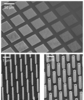
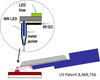
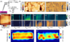
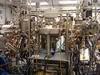
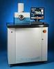
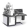
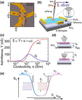
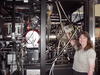
Nanostructures are a critical component of innovations in high performance computing, electronics, energy conservation, renewable energy, biomedical research, and health care. We develop and demonstrate metrology techniques to address nanoscale measurement challenges. These techniques include scanning microwave microscopy, atom probe tomography, transmission electron microscopy, Raman spectroscopy, and time-resolved photoluminescence. Our goal is to push these methods beyond comparative measurements by evaluating absolute uncertainties with cross-method comparisons and calibration techniques that reveal systematic errors. We synthesize semiconductor nanostructures to serve both as test structures for measurement techniques and as building blocks for novel metrology tools and semiconductor devices.
News and Updates
Publications
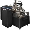
Tools and Instruments
Awards

Press Coverage
TAKING MEASURE BLOG
Contacts
Group Leader and Project Leader Quantitative Imaging
-
(303) 497-5089
Project Leaders (NANOSTRUCTURE SYNTHESIS, CORRELATIVE MICROSCOPY, ATOMIC SCALE CHARACTERIZATION, NANOELECTROMAGNETICS)
-
(303) 497-5069
-
(303) 497-5420
-
(303) 497-5239
-
(303) 497-3997