Summary
Scanning probe technology is an essential tool for measuring nanostructure properties. A major goal in our project is to develop unique probes that combine several functions simultaneously-optical excitation, electrical response from DC to GHz, and morphology.
Description

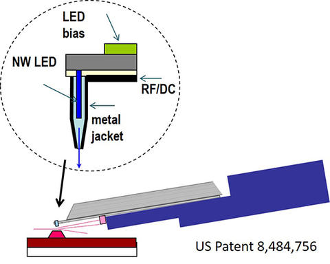
Fig. 1 Schematic illustration of the integrated near-field optoelectronic (INFO) probe showing light emission, microwave reflection lines for measuring specimen conductivity and/or magnetization, and simultaneous contact topography feedback.
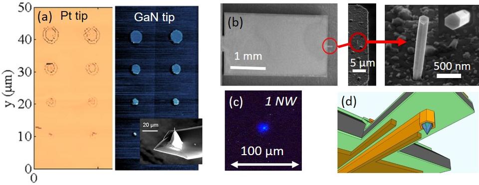
In a collaboration between the Nanoelectromagnetics Project and the Quantitative Imaging Project, we have fabricated and tested a GaN nanowire mounted on an AFM tip as a near-field scanning microwave microscopy (NSMM) tip (see Fig. 2(a) below ). A tungsten atomic layer deposition (ALD) coating provides a microwave pathway to the tip/sample interface. The microwave reflection coefficient S11 for scans over Au microcapacitors on SiO2 steps is shown. The overall S11 contrast on the calibration sample is an order of magnitude higher for the ALD-coated nanowire tip than for state-of-the-art commercial Pt tips. Owing to its flexible structure, nanowire probes have also proven to be insensitive to surface contamination during contact-mode scanning across 2D films. The results are described in two recent publications (see lower right.)
The next step in this project was to develop waferscale fabrication of nanowire tips using selective epitaxy. Figure 2(b) below shows successful placement of nanowire tips on whole wafers that are subsequently fabricated into multiple AFM cantilever units.
A third component is the growth and fabrication of single-nanowire LEDs, enabling near-field optical excitation at wavelengths determined by InGaN quantum wells grown into the nanowire structure. Our advances in p-type doping in core-sleeve nanowires and selective epitaxy have enabled growth and fabrication of single nanowire LEDs (Fig. 2(c) below) with sufficient luminescence to be useful. The high index of refraction for the nanowire leads to a large divergence once light exits the crystal, generating a small volume about 40 nm in diameter that experiences intense optical excitation, with fields falling off rapidly at larger distances.
The final step will be to integrate all three functionalities- scanning probe tip, near-field microwave microscopy and near-field illumination. Unlike flood illumination from remote lasers or optically pumped antennae, the sample under test would be stimulated only directly under the tip. The electrical response is then measured by the microwave circuit integrated with the NSMM, which is sensitive to changes in the local electromagnetic properties of the sample such as sheet resistance and capacitance.
Some examples of applications for the simultaneous operation of the multiple functions include measurement of response of individual grains and grain boundaries in photovoltaic materials, identification and mapping of defects and charge states in nanoscale Si circuits, identifying tissue or molecules under force testing with AFMs, and measuring electrical and mechanical response of neurons and other cellular structures to light. The multiprobe concept is covered by U S Patent 8,484,756.


