
Official websites use .gov
A .gov website belongs to an official government organization in the United States.
Secure .gov websites use HTTPS
A lock (
) or https:// means you’ve safely connected to the .gov website. Share sensitive information only on official, secure websites.
Summary
The core activities in this program are the development and application of metrology for quantitative characterization of hetero-structured materials and devices. In the process, we establish accurate, spatially resolved metrology with sub-micrometer/nanometer/atomic scale resolution from DC to 100 GHz, and beyond for devices that are considered to be 5 to 20 years from production or implementation. These measurements have broad-ranging applications from high performance computing devices to next generation power converters to in vivo biology.
Description
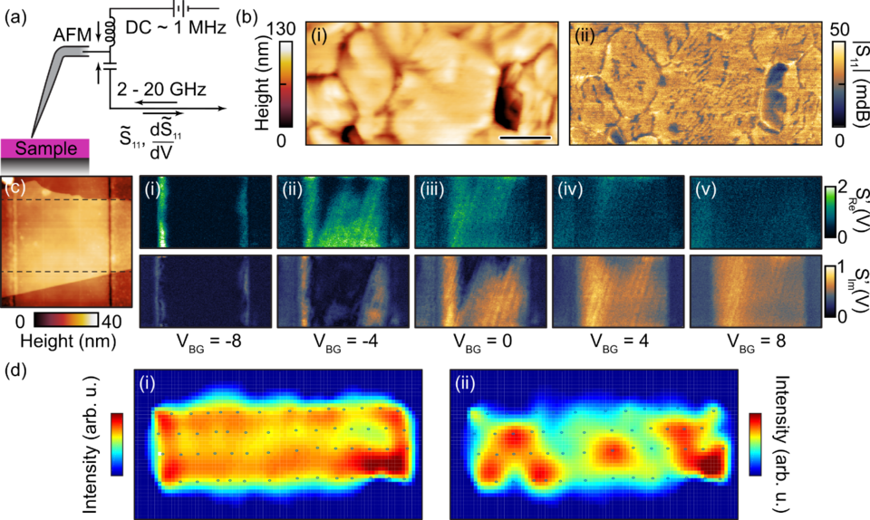
The primary goal of this program is metrology that enables advanced nanoscale device (including electronics, spintronics, and life science) development. Based on current trends in electronics, we are focusing on metrology for two classes of devices: (1) nanoscale devices utilizing and exploring new physics at nanoscale and operating in a broad frequency range (bringing high-frequency to the nanoscale) and (2) devices based on novel materials ( exploring the nanoscale physics in new materials at high-frequencies). Near-field Scanning Microwave Microscopy (NSMM) is the ideal metrology tool for characterizing charge transport, interfacial charge transfer and storage, as well as magnetic properties at the nanoscale. Based on an atomic force scanning probe microscope, a microwave signal is delivered to the ultra-sharp tip and local changes in the tip-sample impedance are measured via the back-reflected complex-valued S11 scattering signal [see Fig. 1(a)]. The technique has nanometer spatial resolution and is sensitive to the local sample permeability, permittivity and the related conductivity, including the free-carrier contribution. A low-frequency or DC tip bias can be applied in parallel to the microwave signal to provide an additional degree of control over sample properties and free charge carriers.
By learning how to fabricate and measure specific devices, we develop metrology that is broadly applicable to whole classes of devices. The electronics research and development community (industry, government, academia) needs the metrological tools we are developing to discern between which high-frequency device paradigms they should pursue and which they should abandon. The impact of these developments on commerce, e.g., the electronics industry could be immense. There are several industrial consortia created just to pursue research of advanced devices. On the one hand they recognize that quantitative measurement will make a major contribution to these efforts. On the other hand, these industrial entities are not able to clearly articulate their measurement needs. In addition to clarifying and providing the measurement needs, our work in this field can enable new functionality that goes beyond "conventional" electronics. Over the course of the next five to ten years, we will be leaders in this field and make an impact in several areas, including electronics beyond complementary metal-oxide semiconductors (CMOS).
Major Accomplishments
Research Highlight
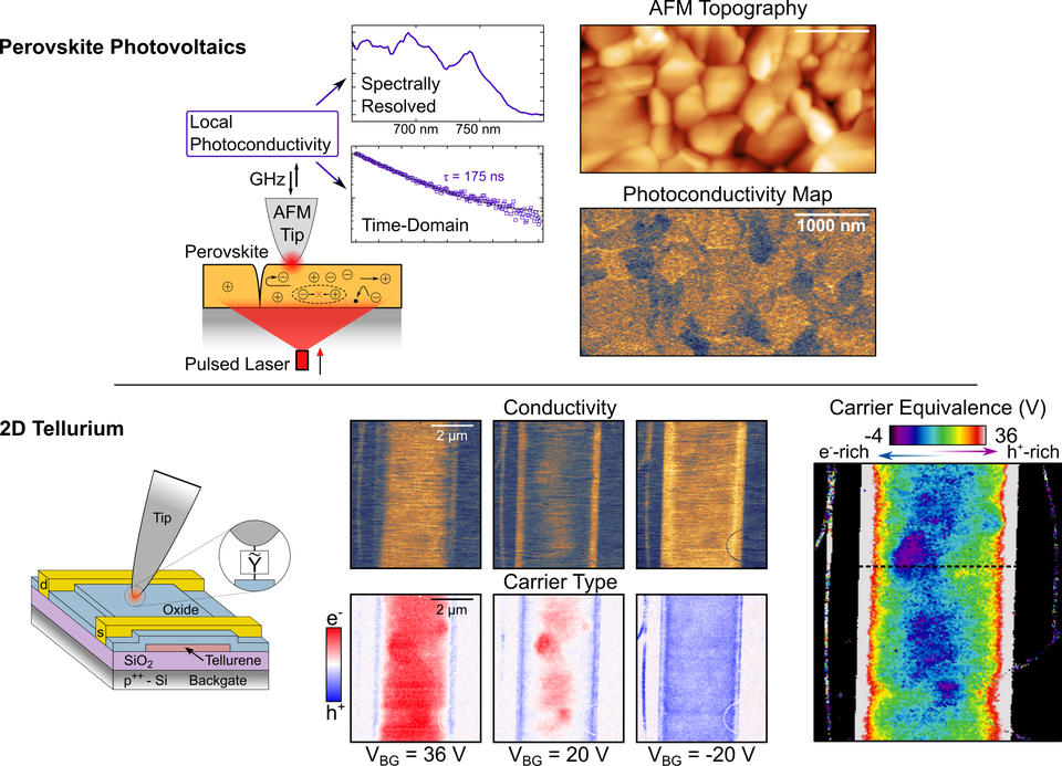
In Figs. 1b-d we show a few examples of NSMM microscopy applications. The measurements of a methylammonium lead-halide perovskite thin film is shown in [Fig. 1b]. The image (i) shows the topography and (ii) the reflection coefficient |S11| of the sample after treatment and deterioration under ambient conditions. An analysis of the image (ii) reveals spatially varying conductivity due to the influence of moisture and associated infiltration of water during film processing and subsequent storage. Fig.1c represent the measurement of a 2D MoS2 device with back-gate bias. Fig. 1c (i) through (v) show the derivative of the resistive (real) and capacitive (imaginary) parts of the reflection coefficient as a function of the back-gate bias VBG. The measured signal reveals a strong variation in the response of the MoS2 free carriers to the backgate voltage both in the local conductivity and capacitance response. The observed stripes in the image correspond to a crystallographic axis of the sample and are likely due to variations in the interaction between molecular layers. Finally, the images in Fig. 1d represent the local measurement of the excited spin wave modes in a 1 micrometer x 3 micrometer patterned 70 nm thick Yttrium Iron Garnet (YIG) element. The image (i) corresponds to the state when no strong excitation is present and (ii) to the spatial distribution of excited modes excited at 6.21 GHz at 180 mT applied magnetic field.
The initial investment in this area has yielded several specific achievements:
- broadband characterization of nanotubes and semiconductor nanowires
- advances in near-field scanning microwave microscopy
- design of capacitance and dopant profile calibration structures for scanning microwave microscopes
- design and fabrication of nanowire-based multifunction probes for scanning microwave microscopy
- characterization of nanoscale materials by scanning microwave microscopy as a function of frequency, temperature, bias voltage, illumination, external magnetic and electric fields, as well as mechanical strain and stress.
- development of complementary ancillary capabilities, which include: modeling of nanoelectronic devices, fabrication of devices in the NIST Boulder clean room, and imaging in the NIST precision imaging facility.
- characterization of magnetic nanoparticles for imaging applications.
- ongoing application of our techniques to virus, protein, DNA imaging, and other life science applications