Official websites use .gov
A .gov website belongs to an official government organization in the United States.
Secure .gov websites use HTTPS
A lock (
) or https:// means you’ve safely connected to the .gov website. Share sensitive information only on official, secure websites.
What are semiconductors?
Semiconductors—materials such as silicon with tunable electrical conductivity—are the base for most electronics, enabling construction of complex integrated circuits, or chips, that power advanced technologies for healthcare, communications, computing, and transportation, among other applications. Demand for chips is already high, and that demand is growing because of uses in emerging technologies such as artificial intelligence, the internet of things and quantum computing.
What is NIST's Role?
NIST has conducted research on semiconductors since the late 1940s, when the field was created by the development of semiconductor devices called crystal diodes for radar during World War II and the invention of the transistor. NIST, then called the National Bureau of Standards (NBS), set up a lab to investigate several related topics, including semiconductors’ electrical conductivity.
The NBS Semiconductor Technology Program was established in 1968 to improve measurement methods, data, reference artifacts, models and theory to enable higher device yields and reliability, lower costs, and improved fabrication and performance. This intensive focus lasted about 20 years.
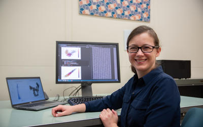
Today, NIST continues its long history of supporting and collaborating with the semiconductor industry, making its own chips for cutting-edge NIST research and partner institutions, and fulfilling more than a century of commitment to responding to national needs.
The State of the Industry
According to the Semiconductor Industry Association (SIA), the U.S. semiconductor industry employs over a quarter of a million workers and company sales totaled $208 billion in 2020. Advances in semiconductor technology have been, and continue to be, a linchpin of U.S. economic prosperity and national security.
But there is currently a global shortage of semiconductors due to several factors, including disruptions related to the COVID-19 pandemic and the increased use of semiconductors in cars. The industry is also facing the technical limits of conventional semiconductor materials. This portends the end of “Moore's Law,” which for more than 50 years has held that, thanks to miniaturization, the number of semiconductor devices called transistors that can be packed on a chip doubles about every two years.
There is also a supply chain problem. Americans invented semiconductors and lead the world in chip technology but provide only 12 percent of global semiconductor manufacturing capacity, according to the SIA. Most chip manufacturing occurs in Asia.
Moves are afoot to boost U.S. semiconductor manufacturing, research innovation and supply chain security. Advances in measurement science, standards, materials, instrumentation, testing, and manufacturing capabilities will be needed to help design, develop and manufacture next-generation microelectronics.
News and Updates

Trump Administration Secures an Additional $100 Billion U.S. Semiconductor Manufacturing Investment for a Total of $265 Billion from TSMC

Department of Commerce Announces Direct Funding Agreement with Bosch for a $225 Million CHIPS Program Award to Support Domestic Production of Silicon Carbide Semiconductors
Department of Commerce Announces Definitive Agreement with I-Pulse for a $250 Million CHIPS R&D Award to Develop Novel Silicon-Carbide Semiconductors
Key Accomplishments
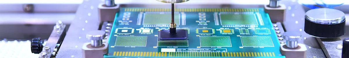
- As chips shrink in size, the semiconductor industry needs increasingly tiny rulers for measuring the widths of circuit features. NIST created an entirely new measurement method to meet this need and in 1979 issued its first photomask linewidth standard, which became an instant best seller. This standard reduced measurement discrepancies among companies tenfold, stimulated the production of new commercial instruments, extended the range of use of optical microscopes, and saved the industry millions of dollars annually.
- NIST is working with the semiconductor industry to overcome approaching physical limitations to chip improvement. NIST partnered with semiconductor companies through the Nanoelectronics Research Initiative (NRI) to identify and tackle the biggest research challenges facing the industry. More than 700 students trained for high-tech professions through the NRI and 60 patent applications were filed based on work leveraging NRI.
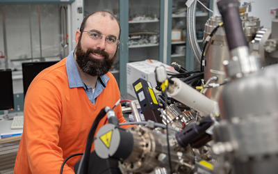
- NIST operates two nanofabrication facilities to produce custom microfabricated devices for its research and measurements to support electrical standards, homeland security, and quantum computing and communications experiments. NIST also makes custom devices for partner institutions. The facilities each house about 50 instruments that lay down very thin layers of materials on silicon wafers, transfer patterns to the wafers, and precisely remove bits of material to make custom chips.
- NIST awarded funds for a research consortium focused on the development of new materials to enable novel computing and storage technologies. NEW LIMITS, for NEW materials for LogIc, Memory, and InTerconnectS, seeks to create innovative solutions that will allow U.S. semiconductor producers to remain on the cutting edge. NEW LIMITS is funded through the Nanoelectronics Computing Research (nCORE) consortium, established in 2017 by NIST and SRCco, a not-for-profit subsidiary of the Semiconductor Research Corporation.
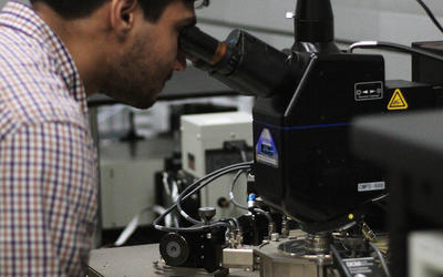
- Among recent research advances, NIST researchers and an industry colleague adapted a novel, low-cost microscopy method to detect nanoscale contaminants during manufacture of semiconductor devices. As chips shrink in size, they become ever more sensitive to contamination, but detecting these flaws is challenging. The Through-Focus Scanning Optical Microscopy (TSOM) technique could easily be incorporated into the manufacturing process for semiconductor devices.
Blog Posts
Curiosity to Career: Encouraging Students to Pursue STEM Education
From Pokémon to Physics: My Journey of Perseverance Into Research