
Official websites use .gov
A .gov website belongs to an official government organization in the United States.
Secure .gov websites use HTTPS
A lock (
) or https:// means you’ve safely connected to the .gov website. Share sensitive information only on official, secure websites.
Nanoscale Mechanical Characterization for Hybrid-Bonding-Ready Structures in Advanced Packaging
- Utilize multimodal atomic force microscopy (AFM) for complementary nanoscale mechanical characterization of materials used in hybrid-bonding structures within advanced packaging.
- Provide elastoplastic material parameters, including elastic modulus, nanoscopic yield stress, and indentation stress-strain curves, to refine processes and enhance predictive manufacturing of hybrid bonding structures.
Since the first computers were developed, their performance has mainly depended on increasing the density of transistors on monolithic chips. However, as we approach the physical limits of transistor scaling, it is becoming evident that we can no longer rely solely on Moore's Law or its extensions. We are now witnessing a revolution in the complex architecture of these chips, with specialized modular components known as chiplets being integrated into larger system-in-package units. This approach enables optimized functionality and enhanced power-per-bit performance, which are essential for high-performance computing, artificial intelligence, and other demanding applications. One significant challenge posed by these advanced packaging technologies is managing the thermomechanical requirements during the heterogeneous integration of various layered stacks and chiplets into new 3D chip architectures.
One of the leading technologies used in the industry for heterogeneous integration in advanced packaging is hybrid bonding. This process involves creating direct metal-to-metal and dielectric-to-dielectric connections, with interconnect pitches measuring just a few micrometers. Due to the small dimensions and the complex thermomechanical processes that these copper pads experience, significant changes can occur in their mechanical and structural properties. Therefore, it is essential to measure these properties to inform the design and fabrication stages and ultimately optimize hybrid bonded integration. This aligns with a beloved NIST expression: "If you can’t measure it, you can’t improve it".
A team led by Gheorghe Stan of the NIST Material Measurement Laboratory has published an article in ACS Applied Nano Materials in which the versatility of a modern Atomic Force Microscope (AFM) was leveraged to provide a variety of valuable nanomechanical measurements for hybrid bonding-ready copper pads.
The AFM is unique in its ability to directly measure the mechanical properties of materials at the nanoscale. This capability enables researchers to examine nanometer-sized surface areas as they undergo various fabrication processes. Changes in mechanical properties provide insights into potential alterations in material structure and serve as a metric for assessing the integrity and reliability of the product.
The NIST team, in collaboration with the Colorado School of Mines (Cristian Ciobanu), George Washington University (Nicolas Alderete), and Intel Corporation (Paresh Daharwal), developed a methodology for using quasi-static and dynamic AFM modes (Contact-Resonance AFM, Single-Step AFM indentations, and Multi-Step AFM indentations) for nanoscale elastoplastic material characterization of SiO2/Cu hybrid-bonding-ready patterns. This is important as the industry wants to have metrology for what they fabricate. “Our work demonstrates that even if we reached the nanoscale critical dimensions, we are ready to perform material characterization at this scale”, said Stan.
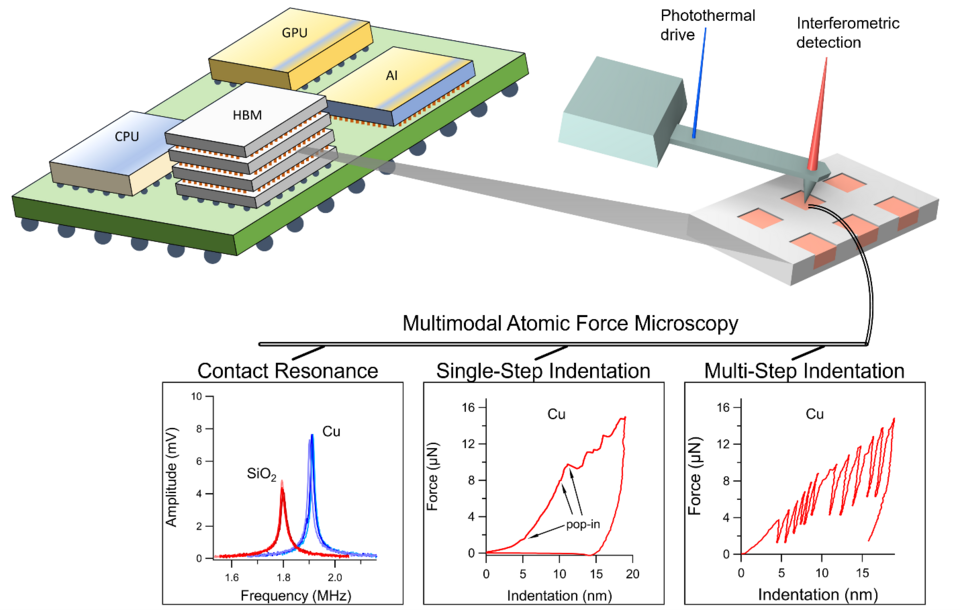
The NIST-led team conducted a study on a specific hybrid-bonding-ready sample by combining high-resolution imaging from AFM with contact resonance and indentation techniques, including single- and multi-step indentation. This approach allowed them to characterize the mechanical heterogeneity of the material, quantify the nanoscopic yield stress statistics, and derive indentation stress-strain curves at room temperature. From their measurements, they clarified the mechanisms of early plasticity and determined the elastoplastic constitutive response of polycrystalline copper. This included key parameters such as elastic modulus, yield stress, and strain-hardening slope.
“The complexity of data analysis is closely tied to the intricacies of the measurements involved,” said Alderete, the lead author overseeing data analysis across all techniques. It is also noted that the measurements were conducted on structures currently of interest to the semiconductor industry, which makes them even more relevant. The materials tested underwent fabrication processes and integration close to the production line. As a result, these types of measurements and the corresponding data are essential for refining processes and enhancing predictive manufacturing of hybrid bonding structures. This work also highlights the efforts of the NIST team to develop AFM-based methodologies that can be adopted by industry to meet their needs for nanoscale material characterization.
The publication was recognized by the semiconductor industry community, with highlights featured on several websites such as Semiconductor Engineering and Chiplet Marketplace.
Note: This work is part of the “Characterization of Nano-to-Microscale Process-Induced Thermo-Mechanical Changes in Heterogeneously Integrated Microelectronics” project, associated with the Grand Challenge 3 of the CHIPS Metrology Program at NIST.
Acknowledgment: This work was performed with funding from the CHIPS Metrology Program, part of CHIPS for America, National Institute of Standards and Technology (NIST), U.S. Department of Commerce.