Official websites use .gov
A .gov website belongs to an official government organization in the United States.
Secure .gov websites use HTTPS
A lock (
) or https:// means you’ve safely connected to the .gov website. Share sensitive information only on official, secure websites.
Gheorghe Stan (Fed)
Physicist
Research Interests
- Develop and customize instrumentation for Atomic Force Microscopy (AFM) to enable advanced and reliable nanoscale property characterization, with direct applications in nanoelectronics, micro- and nano-electromechanical systems, thin film coatings, additive manufacturing, and biotechnology.
- Use AFM-based characterization techniques to investigate nanoscale structure-property relationship in fabricated structures and devices.
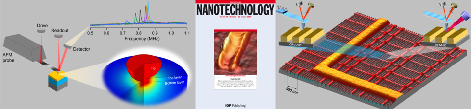
- Develop Contact Resonance AFM (CR-AFM) for nanoscale elastic modulus measurements. Extend CR-AFM to Intermittent Contact Resonance AFM (ICR-AFM) for subsurface and 3D mechanical property measurements.
-
Established collaborative work between NIST, academia, industry, and instrument vendors to promote the development of nanoscale characterization techniques for new materials and devices.
Ongoing Projects
- Nanoscale Property Measurements by Atomic Force Microscopy
- Scanning Probe Microscopy Measurements and Standards
Patents
- US Patent # 9,535,085 "Intermittent Contact Resonance Atomic Force Microscopy and Process for Intermittent Contact Resonance Atomic Force Microscopy," Inventors: Stan & Gates (2017)
Citations
Awards
2009 MSEL Distinguished Associate Award
2021 DOC Bronze Medal “For the invention, development, and industrial application of Intermittent Contact Resonance Atomic Force Microscopy”