Characterization of Nano-to-Microscale Process-Induced Thermo-Mechanical Changes in Heterogeneously Integrated Microelectronics
Summary
Some of the manufacturing difficulties encountered by the heterogeneous integration of modular chips in system-in-package are due to thermal management and mechanical incompatibilities among the various interfaces and building blocks of the package.
This project will provide indentation and scanning probe-based measurements of the thermo-mechanical properties of materials and structures used in advanced packages.
Grand Challenge 3. Enabling Metrology for Integrating Components in Advanced Packaging
Description

Across the entire semiconductor industry, issues related to thermomechanical mismatches encountered during packaging are limiting factors in the design and fabrication of 3D modular integrated circuits.
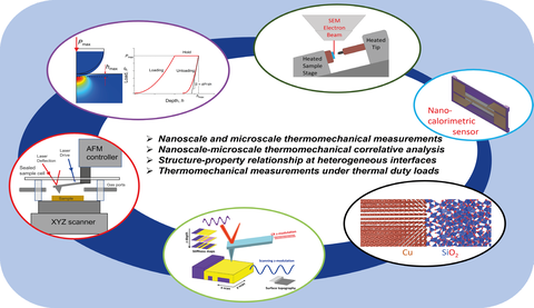
This project will develop novel and necessary metrologies for thermomechanical properties of materials and components used for advanced packaging of future electronics. The macroscale techniques currently employed to determine thermomechanical properties provide inadequate data, as they do not have the spatial resolution necessary to extract local variations at the microscale and do not allow the replication of the real-world thermal load history experienced by materials and components during the actual packaging process.
Building on NIST’s decades-long expertise in nanoscale to microscale mechanical property measurements on microelectronic materials, this project will improve and deliver measurement methodologies and data to industry to enhance their predictive manufacturing.
Currently, there are no established methods to perform precise and accurate nanoscale to microscale thermomechanical measurements. The techniques developed in this project will give engineers the ability to predictively model the packaging process and adapt the packaging design, reducing the need for design by trial-and-error in future packages.
The project capitalizes on more than a decade long interaction with the semiconductor industry, and it is going to continuously improve and extend in terms of measurements and applicability to new classes of materials and components.

