
Official websites use .gov
A .gov website belongs to an official government organization in the United States.
Secure .gov websites use HTTPS
A lock (
) or https:// means you’ve safely connected to the .gov website. Share sensitive information only on official, secure websites.
A novel, low-cost method detects nanoscale contaminants during manufacture of semiconductor devices
An optical microscope does the job
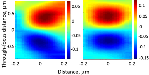
Two composite pictures, each using the TSOM method, show a single nanocontaminant on a semiconductor sample, recorded at several different distances from the lens of an optical microscope. Red indicates highest intensity of scattered light, blue the lowest.
As computer chips and other electronic devices continue to shrink in size, they become ever more sensitive to contamination. However, detecting the nanoscale equivalent of a water spot on a window is incredibly challenging. It is essential, though, since these nearly invisible defects may interfere with proper functioning of these components.
Researchers at the National Institute of Standards and Technology (NIST) have now adapted a low-cost optical method of examining the shape of small objects so that it can detect certain types of nanocontaminants smaller than 25 nanometers (nm) in height—about the size of a small virus. The technique could easily be incorporated into the manufacturing process for semiconductor devices, said NIST researcher Kiran Attota.
At NIST, Attota helped pioneer the method, known as Through-Focus Scanning Optical Microscopy (TSOM), about 15 years ago. TSOM transforms a conventional, inexpensive optical microscope into a powerful three-dimensional shape-measuring tool at the nanometer scale. Instead of recording a single, sharp image when a sample lies at a fixed distance from the lens, the microscope takes several out-of-focus, two-dimensional images, each with the sample at a different distance from the instrument and source of illumination. (Collectively, these images contain much more information than does a single in-focus image.)
A computer then extracts the variation in brightness—the so-called brightness profile—across each image. Each brightness profile is different because for each image, the sample resides at a different distance from the light source. Combining these two-dimensional profiles, the computer constructs a finely detailed, three-dimensional image of the sample.
Indeed, Attota and his colleagues originally developed the technique to record the full three-dimensional shape of small objects, not to detect nanocontaminants. But by optimizing both the wavelength of the light source and the alignment of the microscope, the team produced TSOM images with the high sensitivity required to reveal the presence of nanocontaminants in a small sample of semiconductor material.
Because the optimized TSOM method does not require costly equipment and can image samples in real time, the technique is ready to be adopted by manufacturers, Attota noted.
He and his colleagues, which include Min-Ho Rim, of the SAMSUNG Electronics Co. in South Korea, recently described their work in the Journal of Vacuum Science & Technology B.
Paper: Min-Ho Rim, Emil Agocs, Ronald Dixson, Prem Kavuri, András E. Vladár and Ravi Kiran Attota. Detecting nanoscale contamination in semiconductor fabrication using through-focus scanning optical microscopy. Journal of Vacuum Science & Technology B. Vol. 38, issue no. 5, 050602 (2020), Published online Aug. 28, 2020. https://doi.org/10.1116/6.0000352