
Official websites use .gov
A .gov website belongs to an official government organization in the United States.
Secure .gov websites use HTTPS
A lock (
) or https:// means you’ve safely connected to the .gov website. Share sensitive information only on official, secure websites.
Summary
Relentless, unabated growth of wireless communications technology, and the resulting extraordinary demand for bandwidth has led to the exploration of previously underutilized segments of the electromagnetic spectrum, including submillimeter waves (300 GHz to 1 THz). Breakthroughs in this band will impact a wide variety of technology, including subsurface imaging for biomedical and security applications, space-based communication and spectroscopy, as well as ultra-fast electronics. To fully realize potential technologies that operate at submillimeter wave frequencies, NIST scientists in the Quantitative Nanostructure Characterization Group and the Guided-Wave Electromagnetics Group are researching measurement techniques for characterization of advance materials and on-wafer devices in this band.
Description
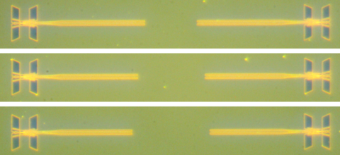
On-wafer calibration test structures for on-wafer, submillimeter wave measurements.
Traditional on-wafer measurement platforms at microwave and radio frequencies rely on probes that make electrical contact to devices under test (DUTs) through direct, mechanical contact. Because of their small dimensions, contact measurement probes in the submillimeter regime are likely to be mechanically fragile and may have a limited lifetime due to repeated cycles of contact between the probe and the DUT. Non-contact probing of on-wafer devices provides an enticing alternative. In place of mechanical contacts, a non-contact probe station utilizes a quasi-optical approach that couples a commercial vector network analyzer (VNA) to DUTs by use of planar, on-wafer antennas.
In collaboration with industry collaborators, NIST is developing measurement techniques, calibration algorithms, and on-wafer calibration test structures for non-contact probing between 500 GHz and 750 GHz. In particular, NIST applies a self-defined, reduced reflectometer calibration for determination of the propagation constant in coplanar waveguide (CPW) devices and de-embed intrinsic DUT properties. Optimized design and fabrication of calibration test structures was found to be critical to suppressing unwanted CPW propagation modes and successful de-embedding of DUT scattering parameters.
Moving forward NIST, in consultation with industrial collaborators, is developing a measurement platform to extend non-contact probing to cryogenic temperatures. This will enable mm-wave probing of superconducting structures below their transition temperature. For example, NIST has developed unique artificial intelligence hardware that can operate at frequencies in excess of 100 GHz, which could potentially be used to detect and classify small signals natively at frequencies above 100 GHz.