
Official websites use .gov
A .gov website belongs to an official government organization in the United States.
Secure .gov websites use HTTPS
A lock (
) or https:// means you’ve safely connected to the .gov website. Share sensitive information only on official, secure websites.
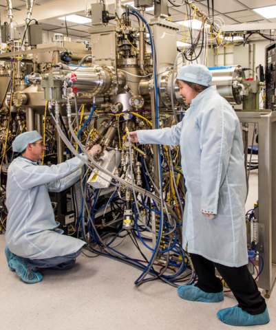
Matt Brubaker (left) and Kris Bertness with the chamber in which nanowires are formed.
One of the persistent challenges in 21st century metrology is the need to measure ever-more-detailed properties of ever-smaller things, from microchip features to subcomponents of biological cells. That’s why, four years ago, a team of NIST scientists patented the design for a nanoscale probe system that can simultaneously measure the shape, electrical characteristics, and optical response of sample regions a few tens of nanometers (nm, billionths of a meter) wide. 100 nm is about one-thousandth the width of a human hair.
Now the researchers from NIST’s Physical Measurement Laboratory are closing in on a working prototype. The newest version of the device, which has a probe tip that functions as an ultra-tiny LED “spotlight,” holds great promise for identifying cancer-prone tissue, testing materials for improved solar cells, and providing a new way to put circuits on microchips, among other uses.
The Integrated Near-Field Optoelectronic (INFO) system has the general configuration of an atomic force microscope (AFM), in which a probe tip on the end of a tiny cantilever beam passes a few nanometers over the surface of a sample, recording exact details of its morphology. But the metal-plated INFO probe also serves as a transmitter that projects microwaves into the sample as well as a receiving antenna that detects the altered microwaves coming back out. The nature of that alteration reveals electrical and chemical properties of the material.
The system uses gallium nitride (GaN) nanowires as the basis of the nanoprobe. “In addition to being a semiconductor, gallium nitride is mechanically very strong,” says group leader Kris Bertness. “It’s a ceramic, kind of like a high-performance kitchen knife. It’s tough as nails.” As a result, the probe – a few hundred nanometers wide at the point and about 4 micrometers (millionths of a meter) long – doesn’t lose its sharpness, which is critical to performance.
But GaN has another major advantage: It is the material widely used in light-emitting diodes (LEDs). So, in addition to serving as an AFM and microwave transmitter/receiver, the probe tip also functions as a light source for measuring how a sample responds to illumination.
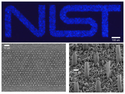
Recently, the team found a way to increase the light output of their probe 100-fold by experimenting with the placement and configuration of “n-type” silicon-doped GaN (which has an excess of free electrons) and “p-type” magnesium-doped GaN, which has a surplus of “holes” – areas where electrons are missing. When an electron and hole combine, they release energy in the form of light, as in LEDs. (See illustration.) Conversely, when light strikes the material in a solar cell, its absorbed energy separates electrons and holes, prompting a current to flow.
“INFO will allow you to illuminate your sample with near-field resolution (tens of nanometers) and also see if the electrical properties of your sample at that exact same location have changed using the microwave sensing method,” Bertness says. “That’s important, for example, in investigating solar cell materials. With this probe, you can see very locally how that conductivity changes when you illuminate it. Similarly, people are working on photodetectors that are based on polycrystalline materials. They would like to know how the grain boundaries differ in their response to light.”
Integrated circuit fabricators could use INFO to look for defects and identify the exact location of specific dopant areas in ultra-small features. “The channels are now getting so small, about 15 nm or smaller, that where the dopant atoms actually sit matters,” Bertness says. “Nobody used to have to care about that, but now they might be able to sense those locations because you could optically excite the carriers in and out of the dopant atoms and sense the change with the microwave reflection.
“Another benefit is that the near-ultraviolet light from the probe tip is very tightly focused, so it can also be used to do much higher resolution lithography than you can do in your standard clean room. In conventional lithography, a beam is directed down at the material surface and directed onto specific exposure areas by using a mask. The INFO probe, however, can use a process called ‘direct write’ that doesn’t require a mask. You could program your probe to move in a specific pattern and coordinate that motion with when the light comes on and off, and you would expose just what you needed.”
There are numerous potential biological applications. For example, there is some evidence that the mechanical stiffness of collagen – the ubiquitous protein that provides support for all parts of the body – may be related to whether cancer cells are more likely to recur or metastasize. “What medical researchers do now is use AFMs to go in and measure the stiffness of tissue,” Bertness says. “But while they’re doing that, they have no way of knowing when the probe is on collagen or something else. INFO might be able to help. Collagen has very interesting, unique optical properties. So, if scientists could illuminate the sample at the same time they’re doing stiffness measurements, they could determine what kind of tissue the probe is over.”
Increasing the LED light output from the probe required a prolonged research effort involving the development of several key capabilities. One of the most difficult problems was developing selective-area nanowire growth, which is a process through which nanowire growth can be prescribed at specified locations. Identification and control over the crystal polarity that develops as the GaN wires grow was found to be critical in developing this capability. Another was determining the right geometry and formation conditions for the p-type section of the probe.
“Initially we tried to fabricate the p-type section as an axial extension of the nanowire probe, however the high-temperature growth conditions required for this type of structure precluded effective p-type doping. In principle, a better p-section could be obtained at lower growth temperatures, however an increased radial growth rate caused nanowires to merge together in our LED test samples,” says project scientist Matt Brubaker. “By synthesizing isolated nanowires via selective area nanowire growth, we could avoid the merging issue and use radial growth to our advantage in synthesizing a core-shell geometry.” After achieving the 100-fold increase in light intensity, “we want to start making these probes and applying them,” Bertness says. “We need to do demonstrations and get some publications out there. That will help us look for potential researchers who could benefit from this technology.”