
NOTICE: Due to a lapse in annual appropriations, most of this website is not being updated. Learn more.

Form submissions will still be accepted but will not receive responses at this time. Sections of this site for programs using non-appropriated funds (such as NVLAP) or those that are excepted from the shutdown (such as CHIPS and NVD) will continue to be updated.

U.S. flag

An official website of the United States government

Official websites use .gov
A .gov website belongs to an official government organization in the United States.

Secure .gov websites use HTTPS
A lock ( ) or https:// means you’ve safely connected to the .gov website. Share sensitive information only on official, secure websites.

Local Electrode Atom Probe Tomography (LEAP)

Local Electrode Atom Probe Tomography (LEAP)
  • Field evaporates (with a voltage and laser pulse) a sharp tip-shaped specimen. Collects the ionization products in a position-sensitive, time-of-flight mass spectrometer 
  • Can determine the atomic species with sensitivity approaching parts-per-million and atomic positions from within the original analysis volume with sub-nm accuracy
  • Manufacturer/Model: Cameca LEAP 4000x Si

Research Highlights:
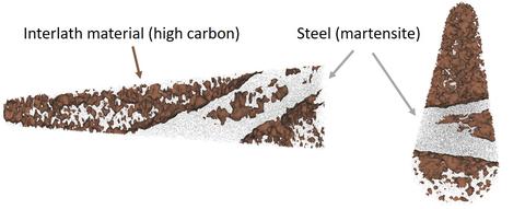
 

Laser-assisted atom probe tomography of weld region showing high-carbon interlath material with an isoconcentration surface of nominally 0.8 at. % embedded in martensite steel.  Image shows a tip from two viewpoints that is mostly interlath material.
Laser-assisted atom probe tomography of weld region showing high-carbon interlath material with an isoconcentration surface of nominally 0.8 at. % embedded in martensite steel.
Credit: Paul Blanchard and Ann Chiaramonti Debay
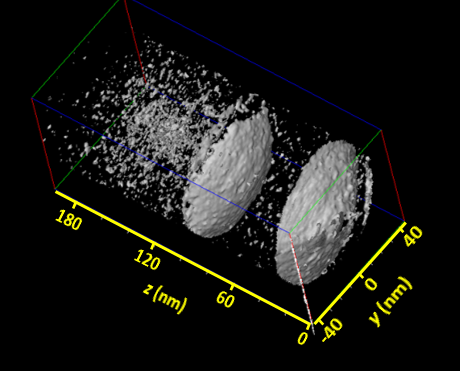
 

Laser-assisted atom probe tomography of InGaN quantum wells in a GaN nanowire grown by molecular beam epitaxy.  Reconstruction with an isoconcentration surface of nominally 0.8 at. % indium is shown.
Credit: Norman Sanford

Customers/Contributors/Collaborators

University of Michigan (Ann Arbor), Colorado School of Mines, University of New Mexico, Lawrence Berkeley National Laboratory, NIST: Quantum Processing Group (687.07), Quantitative Nanostructure Characterization Group (686.09), Nanoscale Reliability Group (647.05)

Created June 8, 2016, Updated April 10, 2023
Was this page helpful?