
Official websites use .gov
A .gov website belongs to an official government organization in the United States.
Secure .gov websites use HTTPS
A lock (
) or https:// means you’ve safely connected to the .gov website. Share sensitive information only on official, secure websites.
Taking Measure
Just a Standard Blog
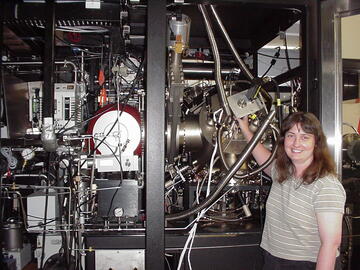
Kris Bertness shows off the crystal growth machine, circa 2000. This system was used to fabricate the compound semiconductor reference materials. It was decommissioned in 2011 when a major component failed shortly before a scheduled move to a new building.
Silicon is the most important semiconductor in the world. It forms the chips that are used for memory and processors in high-end computers, everyday consumer electronics and now in tiny little gadgets that do amazing things.
But there is one thing that silicon cannot do well: produce light. For those devices that emit light, we use a class of materials called compound semiconductors. These materials incorporate two, three or even four atomic elements alloyed together to form a crystal. Varying the alloy composition changes the exact color of light emitted. The earliest of these semiconductors to come into widespread commercial use was aluminum gallium arsenide for infrared light emitting diodes (LEDs), often used in remote controls, and red lasers for early CD-ROM drives and telecom systems. Alloys of indium gallium arsenide phosphide form the basis for modern fiber-based telecommunications. More recently, indium gallium nitride semiconductors were developed for visible and blue light emitters, now used in displays, flashlights, LED lighting and Blu-ray Disc players.
Making multiple layers of alloys with different compositions also alters the way electric charge can move through the material, so compound semiconductors are also used for high frequency and other specialty electronics such as cellphone and military communications.
When I first started at NIST in 1995, my job was to do research on crystal growth of compound semiconductors. By crystals, we don’t mean a pretty object that is somewhat transparent, but rather that the atoms are arranged in a particular structure. We were growing aluminum gallium arsenide and monitoring the crystal growth by reflecting light off the wafers using a window in the crystal growth chamber. This allowed us to obtain real-time feedback about properties such as composition. NIST had a new program at the time promoting collaborations with the optoelectronics industry, which includes all the laser diode and LED manufacturers. I suggested that the community might benefit from standard reference samples that would allow manufacturers to determine the composition of their aluminum gallium arsenide more accurately.
NIST runs an entire program of standard reference materials (SRMs) that cover everything from steel to peanut butter. In my case, these reference samples would be a thick film of aluminum gallium arsenide with its composition specified to high accuracy on top of a thicker semiconductor substrate. There were already many methods for determining the composition, including measuring the color of light that the material emitted or the crystal spacing of the atoms, but these methods were best at comparing two similar samples to identify which one had more aluminum in it. In a manufacturing environment, testers could confirm that their process had drifted to produce material that was now slightly too rich in aluminum. But these methods often did a poor job of getting the correct absolute value of composition. I argued that If NIST provided a standard, everyone could put their measurements on the same absolute scale.
I consulted with people I knew in the industry, and they were quite interested in having these standards available for quality control in the manufacturing processes and to improve basic studies of aluminum gallium arsenide by putting research data on a uniform composition scale. These basic studies are used to model the operation of the semiconductor device in order to save development time on new products or to understand product limitations.
Based on this encouragement from industry, NIST started work on the project in 1998. Doing things to NIST standards meant developing multiple techniques with uncertainty evaluations and storage condition tests. It took a while. Seven years later, in 2005, we delivered our first set of 29 units with one aluminum gallium arsenide composition to the NIST Standard Reference Materials office. In the next year, we delivered another 12 units at a different composition of aluminum gallium arsenide. We sold a handful of the standards those first years, and then sales went very quiet. One explanation could have been that the telecom industry had gone bust. All my original contacts had either retired or were no longer interested in quality standards and basic studies of materials. I consoled myself with the fact that we had published several quality papers on how to do accurate measurements using multiple methods, and that we had made available to the community some high-accuracy standards should the interest return.
Seven years later, someone from my graduate school research group contacted me about attending a workshop on composition standards for semiconductor materials. I was naturally excited to go. There I reconnected with one of my first customers, Temel Büyüklimanli from Evans Analytical Group (as it was called then) in Sunnyvale, California. Temel told me that Evans was using my aluminum gallium arsenide standards to calibrate a type of measurement called secondary ion mass spectrometry, or SIMS for short. This analysis had become particularly important for a new type of laser with a vertical structure that has some big cost advantages for applications in communications, sensing and medical procedures. Because of the way in which his company was using our reference materials, it didn't need to buy very many of them.
Over the years, I've had a couple of inquiries about the standards, and whether we would be able to make similar standards for other semiconductor alloys. I would explain that we had no plans to expand the program given the history of poor sales of our first one. We also no longer have the characterization equipment used to certify the first batches, and I no longer work with aluminum gallium arsenide, though the capability is still at NIST.
Then, this year, something interesting happened. I got an inquiry from someone at a major optoelectronics company asking about the re-certification of one of the aluminum gallium arsenide standards it owned. It turns out that the company had started to use the reference standards in its quality control program. The company did not reveal the exact nature of its standards use, but we know that it is a major manufacturer of aluminum gallium arsenide LEDs and lasers. I looked at our sales records and found that our SRMs have been sold not only in the United States, but also in the Netherlands, the United Kingdom, South Korea, Singapore and Saudi Arabia, some to academic groups but largely to companies that produce compound semiconductor devices or sell equipment that analyzes them. Four purchases were from new customers in the last three years. It was a wonderful surprise to learn this, kind of like walking into a garden where you had planted some seeds that apparently never sprouted. But then you come back five years later (or 15 years later!) and there's something beautiful blooming.
I decided to go back to that early customer, Temel, to find out more about how his company was using the reference materials. Temel referred me to an article he and his colleagues had published in a professional magazine called Compound Semiconductor on his use of NIST standards. His company is using the material to generate secondary standards that allowed employees to develop detailed models on how impurity and aluminum and gallium atom counts depend on the aluminum composition. They can then correct their data for inaccuracies that occur when the actual aluminum gallium arsenide composition of the layers is unknown. For example, small concentrations of silicon are used to change the electrical conductivity of aluminum gallium arsenide, and without the corrections, the concentration of silicon actually in the layers can be off by a factor of two, meaning researchers can overestimate the silicon concentration to be twice as high as it actually is or, conversely, underestimate it by half. Their model also allows them to determine more precisely how thin the layers are. The model can be applied to routine measurements without direct reference to the standards, but to get the highest accuracy measurements, they do a calibration measurement in the same instrument on the standards (or SRMs) that they have purchased from NIST. When asked about the economic impact to his company, Temel told me that they run between 10 and 100 of these tests per day in their offices around the world. They typically charge over $1,000 for the high accuracy runs and about half that for the lower accuracy runs. Our reference sample anchors roughly $3 million per year in revenue for that company alone. It seems that the SRM’s small sales volume does not reflect its actual impact in the industrial community.
There is a resurgence of interest in building up the U.S. semiconductor industry as a strategic economic and defense security goal for our country. While most of the new focus will be on building up the existing silicon chip industry, manufacturing of advanced electronics that make use of compound semiconductors is also important for many commercial and military applications. Thus, the need for more standards of more varieties of semiconductor alloys (like those I mentioned in the first paragraph) will likely grow.
As it turns out, we have come upon an approach that could potentially enable us to develop new standards more quickly than before and help us keep pace with rapidly changing industry needs. My group is now involved with a new research program that uses a method called atom probe tomography (APT) to identify individual atoms being ejected from a sample. Our team has modified a commercial atom probe instrument to reduce the variations in how different elements are counted when instrument operating parameters are changed. Those variations have traditionally made it hard to get the correct absolute composition. This new program could form the basis for much more rapid development of composition standards or certification of industry samples for them to use as internal standards. I’m excited to see if there is another set of semiconductor standards in my future!
About the author

Related Posts


Comments
A classic composition (standard) with multiple layers accompanied by impactful lyrics that the great (semi-)conductors would love to include in their repertoire!
Thank you! What wonderful work you are doing! Best regards to you and all at NIST!