
Official websites use .gov
A .gov website belongs to an official government organization in the United States.
Secure .gov websites use HTTPS
A lock (
) or https:// means you’ve safely connected to the .gov website. Share sensitive information only on official, secure websites.
Atom Scale Device Group
Develops, measures, understands and exploits quantum and electronic devices and sensors at the interface between atomic and nanoscale solid-state systems. Systems under study include dopant-based and nanofabricated Si devices for quantum technologies, quantum simulation, quantum sensing and charge sensing, spins in nanoscale and atomic scale solid-state systems, and hybrid solid-state systems.
Quantum processing offers tremendous opportunities for computing, simulation and precision metrology that greatly exceeds the bounds of what can be done now. Taking advantage of quantum processing is most natural and effective with small, atom-scale devices, for example with cold neutral atoms or charged ions. Most recently, exciting progress has been made implementing quantum computing and simulation with dopants in Si. The dopants serve as atom-scale qubits or sites for the lattice of an analog simulation while Si provides the extremely low-noise environment needed for quantum processing. Just as important, dopant-based quantum devices made in Si can be directly integrated with traditional Si electronics and photonics, providing a path to scalability that can take full advantage of the highly developed Si electronics industry.
Summarizing our program, we are
- Exploring the fundamental operation of electronic and quantum solid-state devices and sensors at the atom-scale through precision metrology of single electrons and spins on deterministically placed atoms,
- Developing foundational knowledge, measurements, and fabrication methods needed to enable nanoengineering solid-state devices and systems,
- Defining and exploiting the operation of atom-scale solid-state quantum devices, simulators, and field-deployable electrical standards and
- Using atom-scale quantum devices to reveal new, unexplored emergent quantum behavior at the limit of single quantum devices, single electrons, single photons and single spins.
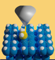
In the Atom-scale Device Group, we are realizing the potential of dopant-based quantum devices in Si. We are developing the tools to do perfect placement of dopants in Si with atom-scale precision. We are extending this to include acceptors as well as donors. We are using these tools to fabricate dopant-based qubits for quantum computing and lattices of dopants for analog quantum simulation. We are developing ways to automate the dopant placement to push toward robust manufacturability of dopant-based devices that could be transitioned to industry. We are investigating the operation of the devices we fabricate. In doing so, we must develop new metrology that will provide the needed initiation, control and readout for the quantum processing.
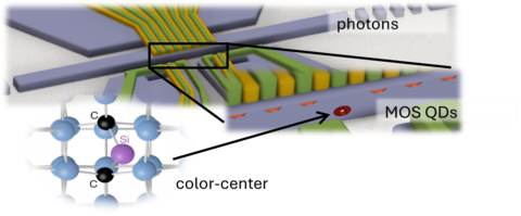
Long-range quantum communication between solid-state qubits, such as atom-scale dopant-based and nanoscale quantum dot qubits, is a critical challenge for implementing quantum processing in the solid state. We are studying color centers in Si that will be used as transducers of quantum information between stationary qubits in a circuit and flying photonic qubits to communicate quantum information between circuits. In addition, color centers have shown potential for use as single-photon emitters. We are investigating this as well.

Precision electron counting is important for the quantum devices we fabricate and study. Knowing and manipulating the charge is essential for quantum device operation. We are exploiting single-electron metrology provided by charge-pumping with quantum dots for measurement and control of device operation. Furthermore, we are utilizing single-electron pumping to develop a quantum current standard that can be deployed to industrial and standards customers. Deployable standards require large enough currents to be straightforwardly measured. Large currents can be achieved using many pumps at the same time. We are solving the materials problems to ensure uniform operation of many pumps, developing the multiplexed operation to run all pumps at the same time, and addressing noise issues that must be overcome so that all of the pumps contribute precisely to the current.
Our experimental programs are strongly supported by our core competence in theory (Theory: Designing the Nanoworld, and Theory: Turning noisy intermediate scale quantum information processing into practical quantum computing). Our theory is being done to understand the experiments, to develop new metrology for these experiments, and to suggest new experiments to be done. Just as important, our theory effort is pushing the envelope of what is known about operating quantum circuits more generally to develop the error mitigation techniques that will push noisy intermediate scale quantum processing to useful quantum computing, simulation and sensing.
News and Updates


Projects and Programs


Publications
Awards

Contacts
Group Leader
-
(301) 975-2595
Group Office Manager
-
(301) 975-5677