
Official websites use .gov
A .gov website belongs to an official government organization in the United States.
Secure .gov websites use HTTPS
A lock (
) or https:// means you’ve safely connected to the .gov website. Share sensitive information only on official, secure websites.
Summary
Much of metrology relies on or would benefit from precision counting. Time and frequency standards, length, and electrical standards all rely on counting. However, despite the importance of these metrologies in information technology, precision counting of individual electrons remains very challenging. Single electron devices (SEDs) count charge through their extremely high sensitivity as charge sensors and the ability to clock individual electrons (or holes) one-by-one through the device at a tunable frequency. This is the basis for a quantum standard of the Ampere. At the same time, these abilities form the basis for a new computing paradigm where quantum states of single electrons can be exploited by generating superposition and entangled states. In the Atom-Scale Device Group, we are working to deliver on-chip, on-demand single-electron sources and sensors for realizing a deployable quantum current standard and for foundational metrology of future quantum computers, sensors, and networks. To do so, we are working to integrate and operate large numbers of devices together in parallel and to identify, quantify and mitigate the effects of noise, especially when many devices must all run perfectly at the same time.
Description
Atoms are natural high-fidelity standards. They are used as the basis for time and frequency standards as well as qubits in nascent quantum computer architectures. Electrostatically defined, single-electron devices behave as tunable artificial atoms which can trap, manipulate, and shuttle electrons deterministically. When operated as a shuttle, SEDs produce a highly accurate DC current, I = eƒ, where ƒ is the frequency of operation. When the device is operated so that one or a few electrons are trapped, the electrons’ spin can be coherently manipulated to form a qubit.
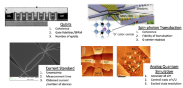
While single-electron sources and high-fidelity qubits exist, the current produced through a few devices is too small to be practical as a deployable current standard and the number of integrated qubits is too small for general purpose quantum computation. The solution to both problems is integration of multiple, reliable, possibly heterogeneous devices on the same chip operating in parallel. In both cases, this straightforward solution is broadly limited by noise. Here noise takes the form of device-to-device variations, drift, and less-than-perfect fidelity to their intended operation, be it charge pumping or spin manipulation. Moreover, single-electron device reliability and noise mitigation are core to success in both Analog Quantum Simulation and Spin-Photon Transduction (see Figure 1).
Realizing the Ampere
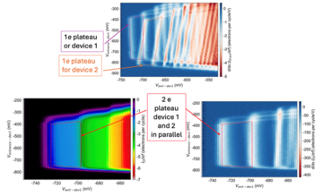
Hundreds of single-electron charge pumps on the same chip, operating perfectly in parallel are needed to realize a large enough current for current standard to be deployed where it is needed in the field. This is a challenging problem with many issues to solve. We are identifying the best material with ease of fabrication, low variability from device to device and low noise. We are developing and implementing circuits and metrology to operate and precisely measure hundreds of pumps operating in parallel at the same time. Ways must be developed to tune away any device-to-device variation. We have done initial work on MOS devices but are now focusing on the more promising Si/SiGe platform. While we work to adapt our fabrication and parallelized device design from the MOS platform to the Si/SiGe platform, we are working to measure devices from collaborators. These measurements inform our device design and point to improvements which can be made in the measurement platform. Moreover, as shown in figure 2 with two devices fabricated by our National Physical Laboratory collaborators on the GaAs platform, we demonstrate the promise of parallel operation at a small scale. These measurements combined with measurements on our Si/SiGe devices from our industry collaborators, reveal a path forward to a more optimal device design for realizing the Ampere in the Si/SiGe material platform.
Noise
Noise-induced device drift reduces the nominal operating time and fidelity for single electron devices, but its effects are difficult to quantify because the presence of drift invalidates simple approaches to the statistics of the ensemble. Identifying the types of noise processes which are present in a device and on what timescales they are active is essential to developing effective strategies to mitigate the effort and achieve robust, precision charge counting.
In the lab we generally only have access to a few measurements of the noise, but not to a full ensemble. We have developed a way of calculating a time-dependent variance from a single measurement which gives the variance of the ensemble as a function of elapsed time since tuning the device. This technique, which we call the rms drift, allows for simple estimates of the number of devices that can be integrated together from a single measurement of the noise.
With a few other assumptions, we can estimate the uncertainty due to drift in a realization of the quantum Ampere as a function of the noise strength and the number of devices (see figure 3a). Our goal for the relative uncertainty in the quantum Ampere is 10-8 A/A and this plot indicates that, with fast tuning, drift should not limit our uncertainty in 128 devices operating at 500 MHz for a current of about 10 nA.
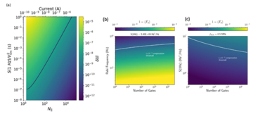
In the other panels of the figure, we show the impact of typical detuning noise in semiconducting qubits on the infidelity of a repeated π pulse operation. This highlights the need to make such pulses fast and to reduce the noise so that many more gates can be run without interruption to compensate for the device’s drift in detuning.
Outlook
Our activities are now focused on showing that a scaling path exists to realize current from a large number of single electron devices. In detail this means designing parallelized devices, bringing online Si/SiGe fabrication in the NIST nanofab, developing automated methods for tuning devices, and methods for addressing individual devices in the array while also holding their operating points. By solving these problems, we will be able to deliver a practical quantum current standard for use in the field, provide single-electron sources that could drive single-photon sources, controllably and simultaneously pump charge to load many qubits in a large circuit or do metrology on all of the qubits at once.