
Official websites use .gov
A .gov website belongs to an official government organization in the United States.
Secure .gov websites use HTTPS
A lock (
) or https:// means you’ve safely connected to the .gov website. Share sensitive information only on official, secure websites.
Summary
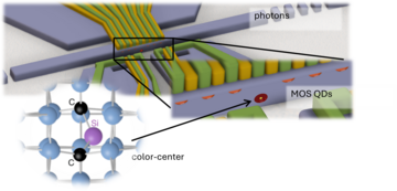
Silicon color centers—optically active, atomic-scale silicon lattice defects—are promising candidates for developing electrically driven, single-photon sources. Moreover, these single-photon quantum emitters can coherently couple stationary silicon qubits, such as spins in quantum dots, with telecommunication flying qubits (photons). This transduction by the color centers provides a means to communicate quantum information between widely separated quantum processors. In the Nanoscale Device Characterization Division, we are synthesizing W and G silicon color centers and pioneering electroluminescence (EL) from color centers in p-i-n diodes to develop electrical single-photons sources to provide photons on demand for precision metrology. We are integrating these color-center point defects into photonic devices to enhance the photon emission and establishing the coherent coupling between color centers and nearby qubits. Our goal is to exploit this transduction to establish long-range quantum-coherent (tele)communication.
Description
Overview: In the first decades of the semiconductor electronics industry, color centers were ubiquitous in silicon. However, through iterative refinement of materials’ processing and spectroscopy methods, color centers are virtually non-existent in commercial silicon today, and leveraging their prospects as quantum light sources or transducers requires deliberately synthesizing color centers in silicon. Non-specific, ensemble fabrication methods for color centers are well established, but the deterministic synthesis and fabrication of electronic or photonic devices aligned to color centers, are both at the technological frontier.
In this program, we are (1) re-examining the process of synthesizing silicon colors centers, (2) developing devices to electrically stimulate color centers as single photon sources, (3) integrating color centers with engineered photonic structures for improved mode matching, Purcell enhancement and optical fiber coupling, and, ultimately, (4) integrating color centers, electron spin qubit devices and photonic devices into one system as a pathway for electron spin-to-photon quantum transduction.
Long term program goal—spin qubit-to-photon transduction via color centers
The long-term goal of this effort is to develop photonic and electronic quantum devices in silicon that are in intimate proximity so that strong coupling can be achieved. We imagine (e.g., Figure 1) that color centers can act as connective tissue, transducing electron spin information by way of spin-to-charge conversion, to a Stark shift in a color center, and thus be encoded in the photon state. Substantial fundamental, materials, and design challenges must be overcome, but the lessons learned along the way have the potential for broad impact and drop-out opportunities for electrically driven single photon sources, optical (projective) readout of silicon spin qubits, and other valuable electron-photon integration capabilities.
Color center synthesis
Initially, we are focusing our efforts on ‘W’ and ‘G’ color centers, which emit at 1218 nm and 1279 nm respectively. Despite being at a shorter than ideal emission wavelength for telecom, the W center is relatively bright and synthesis by silicon ion implantation is well established. However, the W center has a very strict thermal budget, presenting challenges for integrating with electronic fabrication process flows that we are exploring. The carbon-based G center emits in the O-band and has a promising Stark effect for quantum coupling applications but has meta-stable configurational variations that are undesirable and has less developed synthesis protocols while retaining the W center’s fabrication integration challenges. Our future efforts are expected to develop color centers at longer wavelengths, like the C or E color center variations.
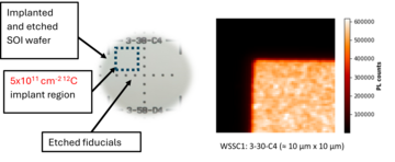
As a starting point for developing both the fabrication and measurement methodology, we prepared color center ensembles in well defined spatial regions on both bulk and SOI (silicon-on-insulator) wafers using masked ion implantation at various ion densities and thermal treatments. We then inspected these specimens using cryogenic, micro-photoluminescence (PL) to compare the evolution of the color centers against the variations, as seen in Figure 2.
Electroluminescence (EL) of color centers via LED integration:
While most color center studies have been done by PL, the need for telecom compatible single photon sources that could be integrated with silicon photonics motivates developing electrically driven color center devices. Color centers are generally unattractive as conventional silicon light sources due to the requirement for cryogenic temperatures (<20 K) to suppress the non-radiative recombination and circumvent the relatively long lifetimes (≈ 30 ns) that limit the emission rates. However, for quantum communications and transduction applications, these liabilities are less significant, particularly when combined with photonic cavity geometries than can reduce the radiative lifetime by an order of magnitude or more. Additionally, materials incompatibility issues between electronic and photonic applications must be resolved.
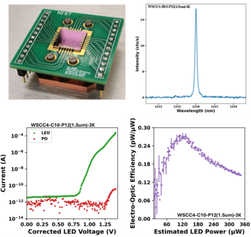
Our team has pioneered the development of both W and G center light emitting diodes (LEDs) by integrating color centers into a p-i-n diode fabricated on SOI wafers for future photonic device integration. Devices and packaging platforms were developed to allow for rapid screening via broad spectrum EL while maintaining compatibility for insertion into high-resolution cryogenic, confocal microscopes for PL vs EL comparisons and hyperspectral mapping of PL, EL and photocurrent. Some published examples of the sample setup, EL from a W center device and measurements of electrical and brightness characteristics are shown in Figure 3.
Engineered photonic structures aligned to color centers:
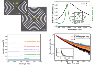
To effectively utilize light generated from silicon color centers, the emitters must be integrated with engineered photonic structures that can enhance light emission and collection into free-space or guided modes. The out-of-plane luminescence studies above suffer from low efficiencies due to silicon’s high index of refraction and poor mode coupling to free-space collection optics located above the sample. By engineering the structure of the silicon and the relative position of the structures to color centers, we can expect dramatic improvements in collection efficiency and emission rates as well as in direct coupling to fiber optics, which relieves the requirements on the measurement apparatus dramatically. Shown in Figure 4 are experiments, done with the Microsystems and Nanotechnology Division, where “bullseye” and “bowtie” optical cavities were fabricated in the silicon around a color center implant region to enhance the W center emitters.
Outlook: Our current activities are focused on isolating single color centers for electrical control, enabling a deterministic, electrically stimulated single photon source, ideally generating indistinguishable photons that will be confirmed via a Hong-Ou-Mandel measurement. In parallel, we are developing strategies for increasing optical collection efficiency through edge launched fiber coupling and vertically coupled fiber grating structures. These paths will be integrated to provide an efficient, electrically driven single photon source. Additionally, configuration options will be improved and fabrication eased by improving the precision of color center synthesis, and we are exploring pulsed laser, nano-ion beam, and nano-masked broad field ion implant approaches to deterministic, localized color center synthesis.