
Official websites use .gov
A .gov website belongs to an official government organization in the United States.
Secure .gov websites use HTTPS
A lock (
) or https:// means you’ve safely connected to the .gov website. Share sensitive information only on official, secure websites.
Summary
One of the first successes of quantum information technology is likely to be small-to-medium-scale analog quantum simulators (AQS). Such simulators will be extremely valuable for solving complex material design problems and a variety of important problems in computational physics and chemistry. Their practical implementation will dramatically speed up drug design, accurate modeling of chemical processes, and find optimized solutions for routing problems. We are utilizing our perfect atom placement to build arrays of phosphorous dopants in Si to use for AQS. We are measuring the response of the arrays to demonstrate their capabilities as AQS and developing new experimental tools to readout the AQS. We are utilizing theory to understand our measurements, define new directions for the experiments and suggest new ways to extract information from these simulations. We are developing an understanding of how these AQS should function and the models that can be simulated (Theory: Designing the Nanoworld and Theory: Turning noisy intermediate scale quantum information processing into practical quantum computing). We are now applying these simulators to address fundamental problems, for example lattice gauge theory, to show that problems that are very challenging to solve by conventional computing can be tackled with AQS.
Description
Why Atom-based Si AQS
Analog quantum simulators are designed quantum systems with a tunable Hamiltonian to emulate complex quantum systems intractable using classical computers due to the exponential growth of the calculations with system size. Simulating strongly interacting fermions (electrons) on a lattice lies at the heart of understanding essential quantum many-body phenomena, such as high-Tc superconductivity, ferromagnetism and spin liquidity, that emerge in solid-state systems at low temperatures.
In the last fifteen years there has been much activity using trapped ultracold atoms and ions, and superconducting circuits to do analog quantum simulation. Although impressive results have been obtained, the physical realization of these AQSs uses atoms to represent electrons, invents artificial interactions to model real interactions, and works at energy scales too hot to model material effects of interest. Recently semiconductor quantum dot arrays and precisely placed dopants in Si have been used for analog quantum simulations of Hubbard models. In semiconductor AQSs, the quantum simulator is a faithful representation of the materials of interest: electrons are used to simulate electronic materials, the real interactions are used, and the energy scales are the same as in the materials being simulated.
AQSs do not require the long-time coherent operation of many qubits or tremendous overhead for error correction. An AQS is simpler because the operation of the analog simulator directly mimics the problem of interest. AQS will be a practical near-term quantum technology. Most importantly for implementation and deployment, semiconductor AQSs can be made on Si chips, exploiting the infrastructure of Si manufacturing and integrable into existing Si electronics, providing a clear path to deployable simulators.
In semiconductor AQS with gated quantum dots, gates are used to tune the quantum dots and the coupling between the dots, an important advantage. Although one-dimensional gated structures and quasi-two-dimensional structures can be fabricated with quantum dots, two-dimensional structures with both internal sites and edge sites can only be realized by dopant placement. Three dimensional arrays of perfectly placed dopants can be envisioned. This means that dopant arrays could be a faithful analog for a wider range of materials and physics problems.
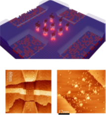
Here in the NDCD we are developing solid-state analog quantum simulators to explore questions in quantum materials and quantum field theory. We use STM lithography to precisely locate individual atoms on a patterned silicon substrate. These atomic structures are then encased in epitaxial silicon, stable in ambient over long periods of time, and can be measured at low temperature in a dilution refrigerator. We have previously demonstrated atomically precise patterning and devices whose performance relies on individual atom placement including a single atom transistor, single electron transistor (SET) sensors used for individual electron charge and spin measurements, RF reflectometry, and the analog quantum simulation of an extended Hubbard model using 3x3 arrays of dopant atoms, that simulate a Hubbard model from a weakly coupled regime to a strongly coupled array.
Fabrication of Dopant Arrays
Advanced hydrogen lithography techniques and low-temperature epitaxial overgrowth enable the patterning of heavily phosphorus-doped silicon (Si:P) monolayers (ML) for use as leads and gates as well as precise positioning of individual atoms with atomic precision. This approach to device fabrication has made Si:P monolayer systems a testbed for multiqubit quantum computing architectures and atomically precise 2-D superlattice designs, whose behaviors are directly tied to the deterministic placement of single dopants. However, continued process developments are needed to reduce dopant segregation and diffusion, achieve perfect atomically smooth surfaces, eliminate defect formation during the encapsulation overgrowth, and reduce uncertainty in the exact dopant placement and number.
Historically, the stochastic incorporation of dopant atoms in patterned lattice sites was limited to a 70% yield for single dopant placement from PH3 (the precursor for P). NIST has developed new methods to improve this incorporation yield, as well as the precision placement of atoms in an array. Using low temperature (4K) STM we have developed a feedback-controlled lithography technique which can reliably remove individual hydrogen atoms from the H-Si(100) surface creating atomically perfect silicon dangling bond patterns into which the phosphine precursor gas can be selectively deposited. A key goal of our current fabrication work is to reliably achieve atomically precise single-dopant arrays.
To improve repeatability, we are now developing low-temperature (4 K) Feedback-Controlled Lithography for improved lithography accuracy combined with AI to perform error detection and correction of the lithography process at the atomic scale. We now can use tip induced dopant incorporation in the lattice to replace the current thermal methods and improve the yield of incorporated dopants to 100%.
Although we operate in an exceptionally low 1x10-11 torr vacuum in the growth chambers, the slow growth rates of 1 monolayer per minute needed to maintain atomic precision in device geometries results in higher than desired contamination levels. We have identified key improvements in our growth chambers to reduced contamination levels in the overgrowth and fitted two of our multi-chamber STM systems with cryo-cooling. Several of the new cryo-components have been installed and quantitative testing and characterization has begun with promising initial results indicating we can achieve low 1x10-12 torr vacuum levels during atomic device overgrowth.
Implementation of these new procedures using STM-based manipulation with improved crystalline overgrowth will ensure incorporation of single phosphorus atoms into a near perfect silicon lattice. These accurately placed phosphorus atoms at each designated site of an array are in turn coupled to atomically aligned gates for in-plane control and sensing electrodes.
Dopant arrays and the Hubbard Model
The Hubbard model is an essential tool for understanding many-body physics in condensed matter systems. The Hubbard model is central to understanding and predicting the underlying physics in a variety of physical systems from superconductivity and magnetic ordering to the exotic properties of topological insulators. Various experimental platforms that form artificial lattices have been explored for realizing Fermi-Hubbard analog quantum simulators, including optical lattices, ion traps and semiconductor quantum dot systems. For probing fermionic many-body physics, the unique advantages of quantum-dot systems relative to other platforms, such as cold atoms in optical lattices, include a readily achievable low-temperature-limit with respect to the hopping amplitude, easy access to transport measurements, and dynamic control of the chemical potential landscape and filling factors using gates. Artificial lattices of dopants in silicon are a promising method for the analog quantum simulation of extended Fermi-Hubbard Hamiltonians in the strong interaction regime.
We have fabricated 3 × 3 arrays of single/few-dopant quantum dots with finite disorder and demonstrated tuning of the electron ensemble using gates and probed the many-body states using quantum transport measurements. We define the electron ensemble in the array by tuning the chemical potential landscape using in-plane gates and measure the low-temperature quantum transport through the array to probe the charge addition spectrum, resonant tunneling, and the impact of inhomogeneity within the many-body system of the arrays. By controlling the lattice constants, we tune the hopping amplitude and long-range Coulomb interactions and observe the finite-size analogue of a transition from metallic to Mott insulating behavior. We have simulated thermally activated hopping and Hubbard band formation using increased temperatures.
As atomically precise fabrication continues to improve, these results enable a new class of engineered artificial lattices to simulate interactive fermionic models helping to achieve an understanding and the ability to predict properties across a range of new quantum materials. The silicon-based solid-state AQS program is establishing the measurement science and fabrication capabilities at the atom scale to detect AQS operation both locally and globally and in time, setting the stage for industry to bring analog quantum simulators out of the lab and into the real world.
Building Solid-State Quantum Simulators for Applications in Lattice Gauge Theory
Numerical solutions of lattice gauge theories provide some of the most accurate ab initio predictions for the properties of nuclear matter. However, simulating real time dynamics of many-body systems of baryonic matter in nuclear physics remains out-of-reach of state-of-art numerical techniques. Analog quantum simulation of lattice gauge theory provides a chance to bridge this divide in near-term quantum hardware. We propose to build prototype devices that test the potential of these ideas using solid-state quantum simulators that offer unique advantages for quantum simulation of nuclear physics due to the combination of strong interactions, large tunnel couplings, and ultra-long coherence times of locally coupled nuclear spins.
Our new platform for atom-based, solid-state analog quantum simulation has unique application in simulating lattice gauge theory. The origin of the mass of elementary and composite particles is an ongoing challenge in the field of particle and hadronic physics. A spontaneous symmetry breaking of gauge symmetries gives rise to the mass of elementary particles, while spontaneous breaking of a chiral symmetry greatly influences the spectrum of hadrons in quantum chromodynamics (QCD). However, a complete picture of dynamical mass generation, and the connection between chiral symmetry breaking and the confinement-deconfinement phase transition, are yet to be developed. Quantum simulation of quantum field theories provides an avenue to explore nonperturbative, and dynamical phenomena such as quantum phase transitions and mass generation in QCD.
Currently we are fabricating 2x2 plaquettes as building blocks for the proposed quantum simulation of a model with direct relevance to nuclear physics. Our proposal uses a dynamical lattice of coupled nuclear spins and conduction-band electrons to realize a quantum field theory: an extended Jackiw-Rebbi model involving coupled fermions and quantum rotors. Classical simulations of this platform show the feasibility of using precision placed nuclear spins hyperfine coupled to electrons to observe dynamical mass generation and a confinement-deconfinement quantum phase transition in 1+1 dimensions, even in the presence of strong long-range Coulomb interactions.
Sensing and Measurement in AQS Atom Arrays
We currently have multiple low temperature cryostats and dilution refrigerators allowing measurements down to the milli-Kelvin regime needed to access the relevant energy scales. We have low noise transport measurement capabilities with electron temperatures approaching 100 mK. We also have operational, individual site remote reflectometry which enables inner-site array sensing of individual electron movement and measurement of local quantum capacitance. These systems allow for low noise, measurement and manipulation up to the 45 GHz regime.

We have demonstrated reflectometry for remote sensing of electrons allowing high-speed charge sensing, improved rejection of charge noise, and the ability to sense inside an atomic array. We have modeled and optimized RF sampling strategies to minimize effects from individual electron charge noise. Shorter integration times and faster sample rates are now used to improve bandwidth. We found reducing the loss within the matching circuit (higher Q) plays a major role in improving the signal contrast, while impedance matching improves sensitivity to changes in the signal reflectivity.
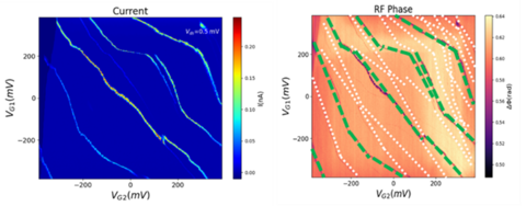
The importance of RF reflectometry versus DC transport is that we can sense individual electron movement within and onto the arrays. As an example, the green dashed lines below show visible charge movement through a 3x3 array in the conductance map below while the white dashed lines (RF signal) show signals invisible in the conductance map that are clearly visible in the RF reflectometry. This demonstrates the ability to sense single electron charge movement and electron reconfigurations inside the array.
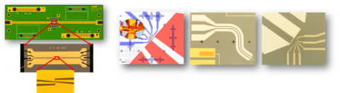
High frequency signal control is needed for coherent electron and nuclear spin manipulation. We use simulation tools to model and design coplanar waveguides (CPW) on the silicon chips and on multi-layer custom low temperature printed circuit board (PCB) with optimized wire bonds to the silicon device chip. The spacing and widths of the patterned waveguides are optimized to have 50Ω impedance at 42.5GHz. S-parameters are carefully simulated to optimize wire bonds and cavity edges of the PCB and silicon chip interface. In the test chip shown below the CPW is terminated with an Oersted line (ESR electron spin resonance drive line) coupled to a symmetrical nanoscale receiving antenna. This new test approach allows design and verification of magnetic field strength at the gap (where the qubit sits) between both drive and sense lines. The novel receiver antenna is a new method that was recently published.
Theory for Atom-based AQS
Experiments on atom-based AQS are challenging. Variations in array structure, even at a single site in a small array, can dramatically change the AQS behavior. Measurements to probe the AQS, for example by transport, are indirect, akin to collision experiments where one measures what is going in and what is coming out without seeing what happens inside the array. Transport experiments can identify the ground state energies for different charge occupations of the array but getting more detailed information is hard and depends on having other gates or an applied magnetic field to perturb the array.
The theory we do can be used to peer deeper into the array, giving us a better chance to understand what is happening in the array and what the experiments are telling us. We have developed and employed simulation tools using exact diagonalization of Hubbard models to find arrays states for sizes up to 4x4. We study much larger NxN arrays using approximate tensor network methods developed to give accurate descriptions of large many-body systems. This theory allows us to identify signatures of various many-body states of the array and determine what to measure to capture these signatures. Our approximate methods allow us to simulate larger arrays to identify when the bulk limit is reached. This is expected to occur in the range of 10x10 arrays when there are more internal sites than edges sites in the array. Applied magnetic fields allow us to better identify spin effects and simulate the onset of complex many-body states, such as fraction quantum Hall states with edge state transport, that are the basis for exotic material behavior currently being studied. Theory will guide experiment as we push our AQS toward these regimes.
Before an AQS experiment can be simulated and interpreted successfully we must know the model that we are simulating: whether it is a Hubbard model with nearest-neighbor hopping, a Hubbard model with longer range hopping, whether the same hopping and energies can be used for every site or are different for different types of sites, or whether the model is limited to on-site interactions or includes longer-range Coulomb interactions. We have developed and used atomistic tight-binding theory, combined with configuration-interaction methods, to study million-atoms models of small arrays with a few electrons. This gives us a more fundamental, atomistic description of the array and allows us to extract the Hubbard models and model parameters that best describe the million-atom system as a small array. We can then benchmark these results by comparing to Hubbard-model parameters obtained by fitting model results to experiment. This gives us the tools to design arrays to target novel quantum, magnetic, or topological physics.