Official websites use .gov
A .gov website belongs to an official government organization in the United States.
Secure .gov websites use HTTPS
A lock (
) or https:// means you’ve safely connected to the .gov website. Share sensitive information only on official, secure websites.
Summary
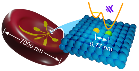
The goal of this program is to achieve complete control over the placement of atoms and molecules for the fabrication, characterization and validation of atom-scale devices in the solid-state, designed to be atomically perfect. Atom-scale devices are the smallest possible solid-state devices (see the figure), representing the final frontier of six decades of downscaling solid-state devices. We are developing the tools to make atom-scale devices by placing one atom at a time, just like laying bricks. We are establishing machine-learning inspired procedures to automate the fabrication, working toward robust manufacturability of atom-scale devices. We are using our tools to create qubits and gates for atom-scale quantum computing, dopant arrays for analog quantum simulation and point defects for quantum sensing and metrology with single photon sources.
Description
For these atomically defined devices, the exact position, type, number of atoms, and their arrangement, dramatically influence device behavior. By controlling the precise atomic makeup and geometry of a device it is possible to engineer a device’s electronic, quantum and mechanical structure to a level where every atom matters.
Atom-by-atom fabrication enables not only the scaling down of traditional devices and electronics to the nano scale, but also provides a precision method for quantum engineering and manufacturing. At this scale the behavior of devices is dominated by the laws of quantum mechanics, which, if well understood within the context of a given device application, can be used to create new, advantageous functionality. Single-atom precision devices allow us to develop this understanding for a variety of systems, some examples being donor spin quantum computers, analog quantum simulators built out of arrays of single atoms, and atom/molecule-based quantum sensors that can be imbedded at the nanoscale.
Physics, chemistry, biology, materials science, and engineering all come together at the atom-scale regime. The ability to reliably fabricate and measure devices of increasing complexity with atomic-precision at the single-atom scale enables unprecedented insights and control over systems of interest to these fields that exist at the ultimate limit attainable for the fabrication of matter.
Engineering atom-scale devices
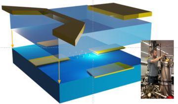
We use bottom-up approaches for atom-by-atom fabrication, combined with traditional top-down (pre/post-) processes where appropriate, to create fully functional atom-scale solid-state devices. For the most critical components, the primary process uses a scanning tunneling microscopy (STM) technique called feedback-controlled lithography and manipulation (FCL/FCM) to position the individual atoms and molecules that will act as key device components on a silicon substrate. These structures are then encapsulated in silicon by epitaxial overgrowth, followed by e-beam lithography and metallization to create micron-scale electrical contacts to the atom-scale device.
The procedure we have implemented for STM-based fabrication (the middle layer of figure 1) proceeds as illustrated in figure 2. Multiple lithographic steps are performed using the STM tip on a hydrogen passivated silicon surface in an ultra-high vacuum (UHV) chamber. Hydrogen atoms are selectively removed to reveal the underlying silicon atoms with exposed dangling bonds, the sites where dopant atoms are placed. In step 1 of the hydrogen depassivation lithography process, the STM is used to create nanometer scale gates or quantum dots that will be used to electrically control single atoms and aid in readout of quantum states of electrons bound to those atoms. In step 2, regions where single atoms will be placed are patterned with nanometer precision relative to the control/readout structuress. In step 3, leads that will provide voltage/current to the central device region are patterned. And finally, in lithographic step 4, those leads are extended out to the micron scale to serve as target pads for creating electrical contact to what will ultimately be an encapsulated device.
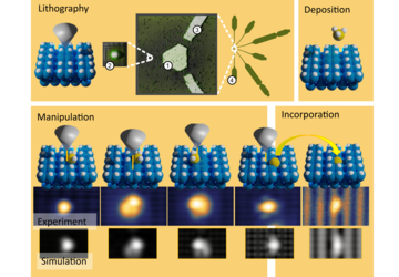
Lithography is followed by deposition in which gaseous precursor molecules are leaked into the UHV chamber. They selectively adsorb only to the STM patterned dangling bond regions. In figure 2, multiple steps of STM tip-based feedback-controlled manipulation are shown in which at each step it is possible to identify the underlying configuration of hydrogen atoms and the precursor molecule on the surface; identification is made possible by simulation of STM images using density functional theory. Once the atom of interest has been isolated, the sample is heated to drive incorporation into the lattice, where the desired atom (phosphorus in figure 2) is substituted for one of the underlying silicon atoms.
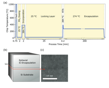
STM-based fabrication is followed by silicon overgrowth which is also performed in UHV. Figure 3 shows this procedure for a delta-layer device. The procedure is the same for STM-patterned devices, where hydrogen passivation and STM patterning occur between the sample flash step and dosing step shown in Figure 3a.
Atom-scale metrology
We develop measurements both ex situ and in situ / operando to characterize devices at both the device-scale as well as the atomic-scale, enabling improvement of process control /material properties and in-depth understanding of device functionality.

We use scanning tunneling spectroscopy to measure the local electronic density of states of quantum structures and devices in situ. Figure 4 shows an example of a cyclic artificial molecule that was created by using the STM to create silicon dangling bonds close to one another. We were able to measure the highest occupied state and the lowest unoccupied state in detail and compare them to an analogous molecule in vacuum. Knowledge of the electronic structure of the device components we create with STM provides us with detailed insights into what quantum functionality they can exhibit as well as act as verification that we have created what was intended.
Once a device has been completed and encapsulated in silicon, it is safe to remove from vacuum. We then make electrical contact to those devices and operate them as intended (e.g. gating and supplying high frequency signals to manipulate spin states) and make measurements (e.g. transport and reflectometry of their quantum properties.
Towards manufacturability
The atom-scale device fabrication process currently requires advanced expertise of the STM operator and takes a great deal of human time to create a single device. This limits both the complexity of devices that can be created as well as manufacturability on any kind of mass scale. A key feature needed to overcome these limitations is automation of the STM-based fabrication process. This poses unique challenges when compared to other fabrication techniques that utilize scanned lithography or deposition (such as e-beam lithography or 3D printing) in two important ways: 1) the necessity for atomic-precision placement of the STM tip requires frequent imaging of the surface and identification/registration of structures such as defects and previously fabricated device elements, and 2) frequent nanometer scale interaction with the substrate causes changes to the tip structure that make identification of imaged structures impossible and undermines the ability to controllably perform lithography and atom/molecule manipulation. These tip changes must be detected and corrected frequently during fabrication.
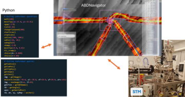
Automation of this process therefore requires implementation of image analysis and artificial intelligence to replace operators who frequently have to make decisions on how to proceed based on items 1 and 2 above. We have developed STM control software to support the intuitive interfacing between the operator and the STM, focusing on atom-scale device fabrication workflow. We are also developing machine vision and machine learning techniques that can be used in place of direct user interaction. Our ultimate goal is that an operator should supply an input file, specifying the strategies for device fabrication, and then the control software and STM would perform all fabrication steps without operator intervention. Our software is developed as open-source on github: https://github.com/usnistgov/ABDNavigator
The primary elements needed for automation that we have identified are STM tip quality control and feature detection (particularly step edges and previously fabricated lithographic features). These form the foundation for more complex logic methods which will allow the automated controller to use images to make “intelligent” decisions to determine progress in fabricating desired structures based on imaging feedback and decide next steps to correct errors or move to other elements of the device. Figure 5 shows the tip-quality control interface (based on work by the Wolkow group in developing machine learning for dangling bond-based devices). A tip-testing region is defined where STM images are acquired to determine tip quality; if the tip quality is not good enough for feature detection and fabrication, then the tip is moved to the tip-conditioning region and gently poked into the silicon surface to reshape it. By repeating this process until the tip images correctly, it is possible to return the tip to a state where it can be used for automated fabrication.
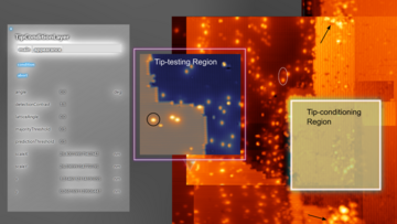
Figure 6 shows an example image from ABDNavigator where the user can plan each fabrication step, how the STM tip will move and where lithography will or will not be performed. Since a device will be created by stitching together multiple regions (defined by the purple boxes in figure 6), we are working on algorithms to image and analyze a region after fabrication, determine lithographic quality, and then move on to the next region to be written, aligning to it using lithographic feature detection.
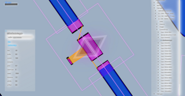
Image analysis and machine learning algorithms are implemented in python and interface with the ABDNavigator software designed with the goal to seamlessly allow either operator control, or automation of each of the needed STM-based fabrication steps (Figure 7).