
Official websites use .gov
A .gov website belongs to an official government organization in the United States.
Secure .gov websites use HTTPS
A lock (
) or https:// means you’ve safely connected to the .gov website. Share sensitive information only on official, secure websites.
Summary
Nano and atomic scale theory of the electronic, magnetic and optical properties of ultrasmall structures, such as semiconductor quantum dots and dopants in Si, the operation of devices made from these structures, and the nanophotonics of these systems is being developed to exploit these structures in quantum technology, metrology and sensing.
Description
Developing and exploiting nanodevices for quantum and nanotechnologies requires nanoscale and atomic scale modeling of ultrasmall structures, devices, their operation, and their response to probes. Key challenges of understanding physics at the quantum/classical interface and measurement at the quantum limit must be addressed. Atomic-scale simulations of the electronic, optical, and spin properties of complex nanosystems are being carried out. These systems include semiconductor nanocrystals, self-assembled quantum dots, plasmonic metal nanoparticles, nanohybrids made by coupling quantum dots with plasmonic structures, and dopant-based Si devices. These simulations provide benchmarks for precise experimental tests of the atomic-scale sensitivity of nanosystems. The work is providing the foundation needed to engineer, build, and understand quantum devices, detectors, sensors, and metamaterials made from these systems. Dopant donor-acceptor complexes in Si are being investigated to determine their potential as manufacturable point defects for use as quantum sensors and single-photon sources.
Key theoretical activities:
Investigating the electronic and photonic operation of atom-based, dopant devices in Si to understand atomic-scale Si quantum devices
- Atomistic tight-binding simulations combined with configuration interaction calculations are being carried out to study million atom models of small dopant arrays in Si with a few electrons. Electronic, optical, magnetic and spin properties of dopant-based devices are being determined to help interpret our analog quantum simulations and define new structures to build and measure. This allows us to explore theoretically large numbers of structures to identify those with interesting or unexpected properties to fabricate and measure.
-
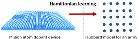 Credit: NIST
Hamiltonian learning: Hubbard models and parameters are extracted from the million atom simulations of small arrays. This provides a way to obtain an atomistic description of the parameters needed to model the analog quantum simulations. This provides a “first-principles” description of the simulators to compare with empirical fitting of Hubbard models to experimental results.
The many-body physics of dopant arrays
-
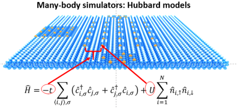 Credit: NIST
Exact diagonalization for small arrays and tensor network approaches for large arrays are being done for extended Hubbard models of interacting electrons to study the many-body states of these arrays.
- The transition to the bulk limit with increasing array size is being investigated to understand how the exotic, bulk material properties of strongly correlated electronic systems evolve from few-electron systems. Novel properties that arise during the transition are being identified and related to what could be seen in our dopant-based analog quantum simulations.
- Ferromagnetism of these arrays is being studied as an example of the many-body physics of strongly correlated systems that could be revealed by our analog quantum simulations. Near half-filling, this is Nagaoka ferromagnetism, that was recently seen in very small 2x2 quantum dot arrays. We predict that Nagaoka ferromagnetism should occur in 3x3 dopant arrays and in larger NxN arrays. This has not been observed yet in larger arrays. We could address this with dopant arrays. For ring arrays, we predict a novel ferromagnetism that occurs for three-electron filling that has not been observed. This provides a target for dopant-based analog quantum simulation that has not been seen in other systems, providing another test of the capabilities of dopant-based analog quantum simulation.
- Different dopant array geometries, straightforward to implement with dopant-based simulators but not necessarily with other simulators, are being simulated to determine what other forms of ferromagnetism for different fillings can be engineered to develop atom-scale dopant-based magnets.
- Transport through these arrays is being investigated to develop observable signatures for the novel correlated states that will allow us to read out the results of analog quantum simulations. Measurements other than transport are being developed to better probe dopant-array simulators. Developing improved read out is a critical step for doing useful analog quantum simulation.
- Different models for describing transport are being developed to best describe actual experiments. This includes treating the sources and drains as small quantum dots to inject single electrons or spins in a controlled manner into an array to investigate how array many-body states respond to an added charge or spin. The use of extended leads to better model typical transport experiments is being tested. The use of quantum jump models to describe a full circuit in an experiment where current flows one way through an array is also being evaluated. The goal is to describe all possible effects on measurements of small atomic scale systems when the measurement apparatus is the same size-scale as the experiment and can be strongly coupled to the experiment.
Theory of dopant complexes in Si: Designing manufacturable point defects for quantum sensing and single-photon sources
- Atomistic tight-binding theory and density functional theory are being used and compared in studies acceptors, like B and Al, and acceptor complexes in Si. This complements previous work done for donors, like P, in Si.
-
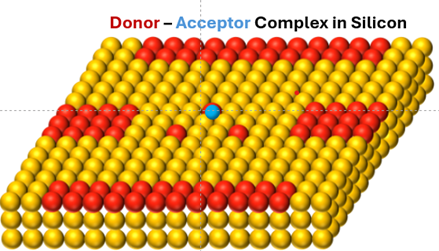 Credit: NIST
Atomistic tight-binding theory and density functional theory are being used study electronic, optical and magnetic properties of dopant complexes of acceptors plus donors in Si. The goal is to understand how the complexes behave when one constituent is a donor with energy levels just below the conduction band and the other is an acceptor with levels just above the valence band. If this level structure persists when the donors and acceptors are strongly coupled in a small complex, then the complex could function as point defect. Our perfect atom placement program can place the individual dopants. This gives us the potential to engineer and fabricate these point defects for applications in sensing and as single-photon sources.
- The use of these engineered dopant donor-acceptor complexes as point defects for quantum sensing and single-photon sources is being explored to identify the most promising candidate complexes. Theory will be benchmarked with experiment to validate the predictive power of theory. It is more efficient to do large-scale searches over different complexes using theory. Large-scale experimental searches would be too time-consuming.
- Dopant donor-acceptor complexes with applications as point defects that could be fabricated by perfect atom placement will be identified.
Ongoing long-term activities
Atomistic tight-binding theory of quantum dots and nanocrystals
- Electronic and optical response of complex self-assembled quantum dot structures is being calculated. The focus is to engineer quantum dot molecules for all-optical quantum computing.
- Engineering and understanding spin states and spin texturing in self-assembled quantum dots is being done with atomistic-tight binding simulations with magnetic fields. The goal is to understand single-electron and single-hole spin states in strongly confined systems and to develop experimental tests for spatial texturing that arises at the level of a single spin spread across a small quantum dot.
Theory of nanooptics and nanophotonics
- Near-field optical microscopy and the nano-optics of nanostructures has been studied using various methods, such as the boundary element method, to study field localization and enhancement on the nanoscale. This was used to understand ways to beat the diffraction limit with near-field microscopy and to unravel the metrology when there is strong coupling between the sample and the near-field probe.
- The plasmonics of metal nanoparticles has been studied using the boundary element method. Much work has been done to understand the effects of nanoparticle size and shape, coupling between nanoparticles, the effect of nanoparticle separation on this coupling and the enhancement of emission from nanoscale emitters near metal nanoparticles.
- The physics of hybrid quantum dot/metal nanoparticle quantum structures has been investigated to identify the effects of weak/intermediate/strong coupling between a quantum emitter and a plasmonic structure.
- The onset of quantum plasmonics in metal nanoparticles and the transition from classical to quantum response has been analyzed using density function theory. Signatures of the quantum plasmonics have been developed.
-
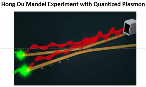 Credit: NIST
Strongly interacting many-electron systems in low dimensions and confined geometries have been investigated using extended Hubbard models for small systems to understand atomic scale quantum plasmonics. Results showed that plasmons quantized as boson excitations emerge in the many-electron excited state spectrum. Signatures to identify quantized plasmons have been developed. Coupling between the strongly interacting many-electron system and quantum emitters reveals the expected Jaynes Cummings ladder of hybrid boson/two-level quantum emitter states. This further confirms the bosonic character of the quantized plasmonic excitations of the many-electron states. Work is underway to simulate a Hong-Ou-Mandel experiment to see how quantum interference proceeds between two quantized plasmons in the many-electron system.