
Official websites use .gov
A .gov website belongs to an official government organization in the United States.
Secure .gov websites use HTTPS
A lock (
) or https:// means you’ve safely connected to the .gov website. Share sensitive information only on official, secure websites.
Summary
To fabricate, measure, and model solid state implementations of atomically precise devices. Develop a robust infrastructure to fabricate prototype few-atom structures in Si, characterize them using low temperature electrical metrology techniques, and model these devices using atomistic and many body quantum physics. Our goal is to fabricate few-atom devices that can operate as coherent qubits or arrayed atomic structures for analog quantum simulation, and to provide the metrology, models, and understanding needed by US industry.
Description
STM patterning at 4K.
This project is developing atomically precise, atom-based electronic devices for use in quantum information processing and analog quantum simulation. We are developing the fabrication, measurement, and modeling methods needed to realize single atom, spin-based qubits in silicon as an integrated solid state, scalable platform. We are also fabricating and measuring arrays of single or few atom clusters for the analog quantum simulation of Hubbard model physics. We use hydrogen-depassivation scanning probe lithography to deterministically place individual dopant atoms in Si. This fabrication architecture enables an array of novel devices such as single atom transistors and solid-state qubits, as well as a path to explore synthetic quantum materials and many-body quantum physics.
The research is focused on advancing the methods for fabrication of atom-based Si electronic structures with improved individual atom precision placement within a silicon lattice. Atomic devices are controlled at the individual atom scale using atomically aligned gates, source, drain, and quantum islands as sensors. These single atom structures are potentially stable for years and can be measured in a variety of low temperature metrology facilities. We use a variety of cryogenic dilution refrigerators and high-frequency/low noise electronics for quantum coherent measurements. The project scope includes scanning tunneling microscope fabrication of atom-scale devices, low temperature electrical characterization, and modeling to obtain a systematic understanding of atom scale device physics.
Major Accomplishments
a. We have developed robust lithography and contact processes that enable routine electrical measurement of atomically precise devices with an emphasis on maintaining atomic-scale device dimensions and properties.
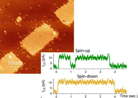
b. We have fabricated and measured a variety of single electron transistors that demonstrate stable coulomb blockade oscillations. We have demonstrated controlled variation in electronic and quantum properties as a function of atomic scale device geometry.
c. We have fabricated and measured a single atom and few atom transistors which show reproducible, stable coulomb blockade oscillations and we have demonstrated controlled quantum properties and spectroscopy at the single atom scale. Our low temperature measurements demonstrate superb charge stability and charge dynamics consistent with simulations.
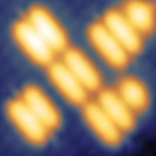
d. We have demonstrated an artificial molecule by creating silicon dangling bonds one atom at a time demonstrating true control of patterning and functionality at the single atom level.
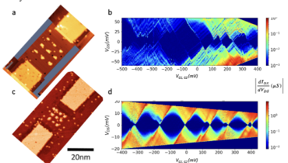
e. We have performed the first analog quantum simulations of an extended Hubbard model using a 3x3 array of few atom clusters in a solid state system. Low temperature transport is used to characterize charge stability, electron filling and probe the many body physics of these arrays in the strong interaction regime.
Recent publications:
- X. Wang, E. Khatami, F. Fei, J. Wyrick, P. Namboodiri, R. Kashid, A. Rigosi, G. Bryant, R. M. Silver, “Quantum Simulation of an Extended Fermi-Hubbard Model Using a 2D Lattice of Dopant-based Quantum Dots”, arXiv:2110.08982, 2021.
- J. Wyrick, X. Wang, P. Namboodiri, R. Kashid, F. Fei, J. Fox, R. M. Silver, “Enhanced Atomic Precision Fabrication by Adsorption of Phosphine into Engineered Dangling Bonds on H-Si Using Scanning Tunneling Microscopy and Density Functional Theory”, arXiv:2112.12200, 2021.
- X. Wang, J. Wyrick, R. Kashid, P. Namboodiri, S. Schmucker, A. Murphy, M. D. Stewart, Jr., and R. M. Silver, “Atomic-scale Control of Tunneling in Donor-based Devices”, Comm. Phys., Nature Research Journal, 3, 82 (2020).
- J. Wyrick, X. Wang, R. Kashid, P. Namboodiri, S. Schmucker, J. Hagmann, K. Liu, M. D. Stewart Jr., C. A. Richter, G. Bryant and R. M. Silver, “Atom by Atom Fabrication of Single and Few Dopant Quantum Devices,” Adv. Functional Matls, Special Issue on Atom by Atom Fabrication, July 2019.
- X. Wang, J. Hagmann, P. Namboodiri, J. Wyrick, K. Li, R. Murray, A. Myer, F. Misenkosen, M.D. Stewart, C. Richter, and R. Silver, “Optimizing Dopant Confinement and Activation in Si:P Atomic Device Fabrication Using Locking Layers,” Nanoscale 10, 4488-4499, 2018.
- J. Hagmann, X. Wang, R. Kashid, P. Namboodiri, J. Wyrick, S. Schmucker, M. D. Stewart, Jr., R. M. Silver, and C. Richter, “Electron-electron interactions in low-dimensional Si:P delta layers”, Phys. Rev. B 101, 245419 June 2020.
- J. Wyrick, X. Wang, P. Namboodiri, S. Schmucker, R. Kashid, and R. M. Silver, “Atom-by-atom construction of a cyclic artificial molecule in Silicon”, ACS NanoLetters, 18 (12) doi: 10.1021/8b02919, 2018.
- J. Hagmann, X. Wang, P. Namboodiri, J. Wyrick, R. Murray, M.D. Stewart Jr., R.M. Silver, and C.A. Richter, “Weak localization thickness measurements of embedded phosphorus delta layers in silicon produced by PH3 dosing,” Applied Physics Letters 112, 043102 (2018).
- S. Schmucker, P.N. Namboodiri, R. Kashid, X. Wang, B. Hu, J.E. Wyrick, R.M. Silver, M.D. Stewart, Jr., “Palladium silicide contacts to subsurface delta-doped phosphorus devices”, Physical Review Applied, 11, 034071, 2019.
- A. N. Ramanayaka, H.-S. Kim, K. Tang, X. Wang, R.M. Silver, M.D. Stewart, Jr., and J.M. Pomeroy, “STM patterned nanowire measurements using photolithographically defined implants in Si(100),” Scientific Reports 8, 1790 (2018).