U.S. flag

An official website of the United States government

Official websites use .gov
A .gov website belongs to an official government organization in the United States.

Secure .gov websites use HTTPS
A lock ( ) or https:// means you’ve safely connected to the .gov website. Share sensitive information only on official, secure websites.

Nanoscale Processes and Measurements Group

Develops measurements that reveal, manipulate and tune the nanoscale physical processes and properties critical to advances in sensors and electronic devices based on quantum materials and utilizing quantum variables.
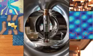
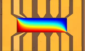
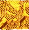
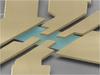
The Nanoscale Processes and Measurements group develops and uses world-leading technology to probe the fundamental properties of novel quantum systems. Our work has applications in quantum information science, electrical standards development, and the advancement of scanning probe measurement techniques. We focus on condensed matter systems, including topological materials, correlated oxides, and moiré materials. We utilize a variety of low-temperature scanning probe techniques, transport measurements, and theoretical annlysis to uncover the electronic properties of these systems.

News and Updates

Projects and Programs

Designing Advanced Scanning Probe Microscopy Instruments

Ongoing
SPM is a general acronym for various probe instruments. The "P" in SPM stands for various types of probe measurements, such as capacitance (C), force (F), tunneling (T), etc. The scanning tunneling microscope (STM), including custom designs at the CNST, uses the quantum mechanical principle of

Electron Spin Resonance at the Single Atom Level

Ongoing
To study electron spin resonance (ESR) on single atoms requires a tool that can probe at atomic length scales. The scanning tunneling microscope (STM) is ideally suited for this, using a tunneling current to probe surfaces. To implement this ESR-STM combination, we send a radio frequency (RF

Engineered Designer Lattices for Quantum Systems

Ongoing
Exposing the low-dimensional materials to a superlattice periodic potential is an effective way to engineer their electronic and other solid-state properties. One example is the moiré superlattice, created by stacking two-dimensional layers at a twist angle, which leads to novel band structures and

Graphene

Ongoing
Two remarkable features of graphene that are opening avenues to multiple applications are its high transport carrier mobility and the broad tunability of its electronic properties. Graphene charge carriers can be tuned continuously from negative carriers (i.e., electrons) to positive carriers (holes

Publications

Detection of fractional quantum Hall states by entropy-sensitive measurements

Author(s)
Nishat Sultana, Robert Rienstra, K Watanabe, T Taniguchi, Joseph Stroscio, Nikolai Zhitenev, D Feldman, Fereshte Ghahari Kermani
Measurements of the thermopower of a clean two-dimensional electron system is directly proportional to the entropy per charge carrier1 which can probe strongly

High-endurance bulk CMOS one-transistor cryo-memory

Author(s)
Alexander Zaslavsky, Pragya Shrestha, Valery Ortiz Jimenez, Jason Campbell, Curt Richter
Previously we reported a compact one-transistor (1T) 180 nm bulk CMOS cryo-memory with a high 10^7 I_1/I_0 memory window and long 800 s retention time based on

Awards

2024 APS Fellow - Curt A. Richter

For pioneering studies of nanoelectronic devices based on advanced materials, including semiconducting, molecular, quantum, and topological

Press Coverage

A new quantum ruler to explore exotic matter

Tech Explorist
These materials, known as moiré quantum matter, can transform into superconductors with zero electrical resistance, perfect insulators, or abruptly produce

Contacts

Technical Inquiries:

General Information

Was this page helpful?