
Official websites use .gov
A .gov website belongs to an official government organization in the United States.
Secure .gov websites use HTTPS
A lock (
) or https:// means you’ve safely connected to the .gov website. Share sensitive information only on official, secure websites.
Summary
The transmission of information in today's electronics requires the movement of electrical charge, which expends energy and generates heat, creating two limitations that are impeding the development of new technologies. Future electronics may overcome the limitations of using electron charge as the main information carrier by instead using electron spin, where the electron acts like a small magnet which can point in different directions. Research into transmitting the spin information from one place to the other without moving charge is sometimes referred to as spintronics. Topological insulators (TI) are a new class of materials with promising spintronic applications. They behave as an insulator in their bulk interior while possessing metallic surfaces, thereby permitting charges to move only on their surfaces. In the bulk, TIs have an energy gap separating the conduction and valance bands, similar to an insulator. On the surface there are special surface states that lie within the bulk energy band gap and permit metallic surface conduction. In the TI surface states, the electron spin always points perpendicular to the direction the electron is traveling. This spin-locking mechanism gives rise to reduced scattering of the charge carriers and possible applications to spin-related electronic devices. The goal of this project is to characterize the metallic surface states of topological materials with atomic scale resolution and determine their special electron spin properties for use in new spintronic device applications.
Description
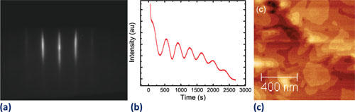
A family of TI materials can by synthesized by combining binary compounds of Bismuth (Bi) or Antimony (Sb) with Selenium (Se) and Tellurium (Te) to form Bi2Se3, Bi2Te3, and Sb2Te3 compounds. In these material compounds the spin of the electron has a strong interaction with the motion of the electron, giving rise to what is called a large spin-orbit coupling. This results in a shift of the electron energy levels with the consequence that these materials become topological insulators. Our efforts to synthesis these materials include molecular-beam-epitaxy (MBE) growth of thin films, and furnace growth of 3-dimensional crystals. In the MBE method, CNST researchers heat up Knudsen cells containing the various elements. The elements then evaporate and combine as they condense on a substrate. Reflection-high-energy-electron-diffraction (RHEED) measurements are used to monitor the quality of the growing film (Fig. 1(a)). Each oscillation of RHEED intensity in Fig. 1(b) corresponds to the growth of one "quintal" layer consisting five repeating atomic layers of the material. Figure 1(c) shows an atomic force microscopy image of an MBE grown Sb2Te3 thin film. Current efforts are focused on growing TI films directly into electrical device geometries for atomic scale characterization with gating tunneling microscopy measurements developed in CNST. These TI device measurements will allow researchers to determine the conductivity and spin related properties of the TI surface states for future use in spintronic devices.
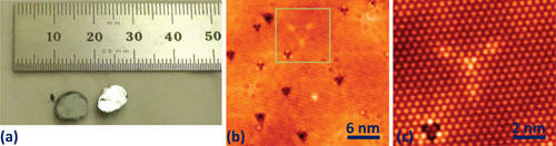
Bulk 3-dimensional TI crystals are synthesized by combining the individual chemical elements in a high temperature furnace to form a melt, which is then cooled very slowly to anneal out defects. High quality crystals of Bi2Se3 and Sb2Te3 have been grown in CNST (Fig. 2(a)). Atomic scale characterization measurements are performed by cleaving a piece of the bulk crystal in ultra-high vacuum and performing scanning tunneling microscopy measurements. Figure 2(b) shows a 30 nm x 30 nm image of the surface of a cleaved Sb2Te3 crystal. A variety of surface and bulk defects can be observed as electronic distortions in the periodic Sb2Te3 lattice. Fig. 2(c) shows a blow up of two defects in Fig. 2(b). Understanding how such defects affect the transport of metallic surface carriers and how they can potentially change the electron spin direction is central for future device applications.
Selected Publications
- Creating nanostructured superconductors on demand by local current annealing, H. Baek, J. Ha, D. Zhang, B. Natarajan, J. P. Winterstein, R. Sharma, R. Hu, K. Wang, S. Ziemak, J. Paglione, Y. Kuk, N. B. Zhitenev, and J. A. Stroscio, Physical Review B 92, 094510 (2015).
NIST Publication Database Journal Web Site - Quasiparticle scattering from topological crystalline insulator SnTe (001) surface states, D. Zhang, H. Baek, J. Ha, T. Zhang, J. Wyrick, A. V. Davydov, Y. Kuk, and J. A. Stroscio, Physical Review B 89, 245445 (2014).
NIST Publication Database Journal Web Site - Electric field tuning of the surface band structure of topological insulator Sb2Te3 thin films, T. Zhang, J. Ha, N. Levy, Y. Kuk, and J. Stroscio, Physical Review Letters 111, 056803 (2013).
NIST Publication Database Journal Web Site - Experimental evidence for s-wave pairing symmetry in superconducting CuxBi2Se3 single crystals using a scanning tunneling microscope, N. Levy, T. Zhang, J. Ha, F. Sharifi, A. A. Talin, Y. Kuk, and J. A. Stroscio, Physical Review Letters 110, 117001 (2013).
NIST Publication Database Journal Web Site - Scanning tunneling microscopy of gate tunable topological insulator Bi2Se3 thin films, T. Zhang, N. Levy, J. Ha, Y. Kuk, and J. A. Stroscio, Physical Review B 87, 115410 (2013).
NIST Publication Database Journal Web Site