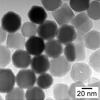
Our group develops and advances optical, electrical, and magnetic spectroscopic measurement methods for nanoscale characterization of materials, light-matter interactions, electro-magnetic and magneto-optical response of matter, charge and energy transfer, and interfacial electronic structure. The multipronged approach leverages much of the electromagnetic spectrum for probing samples with nanoscale spatial resolution and/or sub-picosecond time resolution. We advance techniques with the purpose to uncover fundamental properties of materials and devices such as nanostructured materials, engineered interfaces, quantum-confined structures, among others.
Some of our unique capabilities include:
- Local nanoscale spectroscopy of interfaces and devices
State-of-the-art custom designed scanning probe combining the spatial resolution of atomic force microscopy (AFM) with wavelength tunable lasers and opto-mechanical AFM probes to enable absorption spectroscopy with unprecedented spatial resolution, sensitivity and time resolution. Microscopic and scanned probe Raman spectroscopy to quantify properties of low-dimensional materials.
- Advanced optical techniques for spectroscopy and measurements of dynamics
Tunable mid-infrared and visible/ultraviolet excitation with multichannel mid-IR or Terahertz detectors for time-resolved spectroscopy, hyperspectral imaging, and related nonlinear spectroscopies are used to measure ultrafast dynamics in the condensed phase. Femtosecond optical techniques, including conventional pump-probe, advanced four-wave mixing (multidimensional) spectroscopy, broadband spectral interferometry, multi-harmonic coherent control, and pulse shaping are used to sensitively measure time-dependent effects. Two-dimensional optical coherent spectroscopy reveals how energy states are coupled in materials and can be used to distinguish quantum pathways that underlie light-matter interaction.
- Manipulation of matter on the nanoscale.
Unique physical and chemical characteristics of 2D materials, electrical and optical properties present specific opportunities in electronic and optoelectronic devices, including transistors, photodetectors, light-emitting diodes, and solar cells. Extensive in-house engineering and synthesis capabilities to uniquely make nanomaterials, create advanced 2D heterostructures, fine tune properties and isolate specific parameters for study.
- In situ spectroscopy
In-operando spectroscopic techniques encompass a broad energy, wavelength, temperature, and magnetic-field range. Spectroscopic characterization of dynamics at the nanoscale pervades many of the applications of this group ranging from ultrafast carrier generation and relaxation to slower battery electrode interphase evolution. We have investigated magnon formation, memristor dynamics, plasmons, and energy transfer processes using these techniques.
- Leveraging light-matter interactions for nanostructured materials
A wide portfolio of spectroscopic techniques ranging from spectroscopic ellipsometry to understand optical properties of new materials to THz spectroscopy to extract conductivity and mobility of new materials optically. Internal photoemission (IPE) spectroscopy to measure the band offsets within solid-state nanoelectronic devices.