
Official websites use .gov
A .gov website belongs to an official government organization in the United States.
Secure .gov websites use HTTPS
A lock (
) or https:// means you’ve safely connected to the .gov website. Share sensitive information only on official, secure websites.
Integrated Photonic Circuits and On-Chip Laser
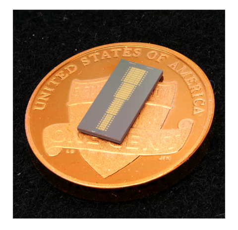
Integrated photonic chip with 32 miniaturized lasers. Coin included for scale.
The Technology
Stable, low-noise lasers have transformed metrology and precision measurements. With the recent emergence of integrated photonic circuits — microchips for light — scientists are interested in integrating lasers with microchips. Miniaturized lasers could give a big boost to emerging technologies such as quantum computers, quantum sensors and field-deployable atomic clocks.
Shrinking lasers has proved challenging, however, in part because photonic circuits are usually deposited on wafers made of silicon, which is not a suitable material for lasers. So while many other technologies have been shrunk to chip scale, lasers and other components such as photodetectors and amplifiers often remain bulky and consume substantial power.
Rather than silicon, so-called group III-V semiconductors are the go-to technology for laser systems. (Group III-V semiconductor materials are made from elements in groups 13 and 15 — formerly groups 3 and 5 — of the periodic table, such as gallium, arsenic, aluminum, indium and phosphorus.) These materials, however, cannot be deposited or grown on silicon because their crystalline structures do not match.
NIST researchers got around this problem by growing semiconductor materials such as indium gallium arsenide on a substrate based on the same material (gallium arsenide) and then chemically bonding it to a silicon wafer.
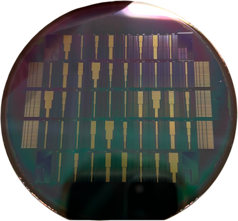
Using this technique, the researchers developed a scalable process for fabricating their lasers on silicon wafers. The process enabled the scientists to use 95% of the wafer’s surface area — a higher yield than any other group has been able to achieve. Maximizing surface area yield is key to reducing manufacturing costs of chip-based technologies.
The researchers were able to fit up to 32 lasers on a chip that’s 5 millimeters by 10 millimeters, roughly the size of the end of a USB connector. Each laser is smaller than 1 square millimeter — no larger than a pen tip or pinhead. They are among the smallest lasers anyone has made in the wavelength range between 700 nanometers and 1 micron — the part of the electromagnetic spectrum where visible light shades into infrared.
Advantages Over Existing Methods
Lasers with wavelengths from 700 nanometers to 1 micron tend to be large and expensive, and they can consume a lot of power. A photonic chip less than the size of a coin with 32 lasers on it will consume much less power and potentially cost less than today’s technology.
Such chips could be ideal for integrating into emerging quantum technologies such as alkali vapor cells and trapped ion systems, both of which are used in many types of quantum computers, atomic clocks and other quantum sensors. Today’s bulky lasers and photonic components often make it hard to create portable, field-deployable versions of these quantum technologies.
Applications
Lasers with wavelengths below 1 micron are essential for emerging quantum systems based on optically controlled neutral atoms and trapped ions. These include quantum computers that use laser light to manipulate atoms and ions used as quantum bits (qubits), the fundamental building blocks of quantum computers, and systems to encode information to be sent over quantum networks.
Many people are also interested in making highly accurate optical atomic clocks that are small enough to fit inside an airplane or vehicle, which could make it possible to navigate without relying on GPS signals and satellite communications. Today’s commercial optical clocks are roughly the size of a small refrigerator and can cost millions of dollars. Chip-scale lasers could help small, portable optical clocks reach their full potential.
Quantum magnetometers, electric field sensors, gyroscopes and accelerometers all rely on lasers to operate. Making these quantum sensors truly chip-scale will require chip-scale lasers. That could lead to numerous new technologies, including mobile units that sense underground minerals or hidden tunnels. NIST researchers’ efforts to develop integrated, on-chip lasers provide a pathway toward compact quantum sensors based on atomic and trapped-ion systems.
Key Papers
Nima Nader, Eric J. Stanton, Grant M. Brodnik, Nusrat Jahan, Skyler C. Weight, Lindell M. Williams, Ali Eshaghian Dorche, Kevin L. Silverman, Sae Woo Nam, Scott B. Papp and Richard P. Mirin. Heterogeneous tantala photonic integrated circuits for sub-micron wavelength applications. Optica. Published online April 24, 2025. DOI: 10.1364/OPTICA.554862
Nima Nader, Eric J. Stanton, Grant M. Brodnik, Nusrat Jahan, Skyler C. Weight and Ali Eshaghian Dorche. Heterogeneously Integrated Distributed Feedback Lasers at 980 nm. 2024 IEEE 29th International Semiconductor Laser Conference (ISLC). Published online Oct. 24, 2024. DOI: 10.1109/ISLC57752.2024.10717343
Nima Nader, Eric J. Stanton, Grant M. Brodnik, Nusrat Jahan, Skyler C. Weight, Ali Eshaghian Dorche, Lindell M. Williams, Kevin L. Silverman, Sae Woo Nam, Scott B. Papp and Richard P. Mirin. Heterogeneous integration of single-frequency lasers at 980 nm. Frontiers in Optics + Laser Science 2024 (FiO, LS). Published online 2024. DOI: 10.1364/FIO.2024.FM5E.2
Nusrat Jahan, Skyler C. Weight, Eric J. Stanton, Ali Eshaghian Dorche, Kevin L. Silverman, Sae Woo Nam, Richard P. Mirin and Nima Nader. Heterogeneously Integrated Near-Infrared Fabry-Perot Diode Laser on Tantalum Pentoxide. Frontiers in Optics + Laser Science 2024 (FiO, LS). Published online 2024. DOI: 10.1364/FIO.2024.FM5E.3
Ali Eshaghian Dorche, Nima Nader, Eric J. Stanton, Sae Woo Nam and Richard P. Mirin. Heterogeneously Integrated InGaAs DFB Laser on Tantalum Pentoxide. CLEO 2023. Published online 2023. DOI: 10.1364/CLEO_SI.2023.SM2J.5
Ali Eshaghian Dorche, Nima Nader, Eric J. Stanton, Sae Woo Nam and Richard P. Mirin. Heterogeneously Integrated Near-Infrared DFB Laser on Tantalum Pentoxide. Optical Fiber Communication Conference (OFC) 2023. Published online 2023. DOI: 10.1364/OFC.2023.Tu3C.6
Key Patents
E. J. Stanton, N. Nader. Wafer bonding method for transferring thin films to a substrate. United States Patent Application US20230402816A1. Filed Jun 9, 2023.
Contacts
-
(303) 497-3746