
Official websites use .gov
A .gov website belongs to an official government organization in the United States.
Secure .gov websites use HTTPS
A lock (
) or https:// means you’ve safely connected to the .gov website. Share sensitive information only on official, secure websites.
Photoconductive Switches

The Technology
The technology for transporting high-speed, high-bandwidth communications signals is improving at a rapid pace — with 5G deployed and 6G technologies on the horizon. With 6G proposed to operate near or above 100 gigahertz (GHz), the communications industry and the electronic test community must prepare to measure these high-frequency signals. State-of-the-art test equipment currently operates up to 110 GHz, so a whole new generation of test equipment will be needed for continuous coverage of 5G and 6G bands.
NIST provides traceability up to 110 GHz for cross-frequency phase (i.e., the relationship between phases at different frequencies) and 75 GHz for power and impedance. Cross-frequency phase calibrations of electronic test equipment are achieved using calibrated photodiodes, which leverage a well-characterized stream of ultrafast optical pulses converted into the time domain. However, commercially available photodiodes are fundamentally limited in bandwidth by two factors: the switching speed/bandwidth of the semiconductor technologies that generate the pulses, and the frequency limit of single-mode operation of coaxial interconnects used to carry the calibration signal from the generator to the waveform measurement instrument. Therefore, NIST cannot depend on commercially available photodiodes to support 6G applications and must develop new ultrafast optoelectronic standards.
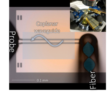
NIST researchers are developing solutions to both problems in a package that could be used as next-generation phase standards. For one, they are creating high-speed photoconductive switches (PCS) that can operate at much higher frequencies than traditional photodiodes. A PCS utilizes the fact that the ultrafast incident light very briefly increases electrical conductivity, enabling ultrafast switching. The NIST team has demonstrated on-wafer photoconductive switches that operate up to 1 terahertz, future-proofing our phase calibration.
To address the connector issues, NIST scientists are at working with state-of-the-art connector technologies as well as developing a chip-scale, on-wafer pulse generator suited to calibrating next-generation connectorless electronics. Circuits operating in an on-wafer environment have been demonstrated at frequencies into the terahertz regime.
Future goals include embedding the PCS devices as pulse generators for quantum science.
Advantages Over Existing Methods
As electronics evolve away from band-limited connectorized devices, on-wafer test methodologies will require an on-chip reference source to characterize those circuits. This could be achieved via a photoconductive switch co-fabricated or bonded to a circuit that would operate as an optoelectronic chip-scale reference pulse generator, where an on-wafer calibration is made and transferred to the device under test through a wafer probe or other coaxial interconnect.
Placing photodetectors (photodiodes, photomixers, photoconductive switches) directly in an on-wafer environment and integrating them with other standards for scattering parameters and power could be used to characterize broadband on-wafer circuits in their operating environments. Thus NIST’s photoconductive switches and other on-wafer characterization would not be limited in bandwidth or operating frequency by coaxial connectors.
Applications
Photodetectors are widely used to characterize the complex frequency response of waveform measurement instruments such as vector signal analyzers, sampling oscilloscopes and light-wave component analyzers. NIST’s high-speed photoconductive switch technology can be used at frequencies up to 300 GHz and beyond. It is expected to be very attractive to high-speed electronics and optoelectronics manufacturers.
Key Papers
Bryan Bosworth, Nicholas Jungwirth, Jerome Cheron, Anna Osella, Franklyn Quinlan, Madison Woodson, Jesse Morgan, Andreas Beling, Ari Feldman, Dylan Williams, Nathan Orloff and Chris Long. Electro-optic arbitrary millimeter-wave sources for THz electronics. Proc. SPIE PC12430, Quantum Sensing and Nano Electronics and Photonics XIX. March 17, 2023. DOI: 10.1117/12.2661190
Bryan T. Bosworth, Nick R. Jungwirth, Kassiopeia Smith, Jerome Cheron, Franklyn Quinlan, Madison Woodson, Jesse Morgan, Andreas Beling, Ari Feldman, Dylan Williams, Nathan D. Orloff and Christian J. Long. Electro-optically derived millimeter-wave sources with phase and amplitude control. Applied Physics Letters. Oct. 11, 2021. DOI: 10.1063/5.0058815
J.A. Jargon, C.J. Long, A. Feldman and J. Martens. Developing Models for a 0.8 mm Coaxial VNA Calibration Kit within the NIST Microwave Uncertainty Framework. 2020 94th ARFTG Microwave Measurement Symposium (ARFTG). Jan. 2020. DOI: 10.1109/ARFTG47584.2020.9071653
A. Mingardi, W-D. Zhang, E.R. Brown, A.D. Feldman, T.E. Harvey and R.P. Mirin. High power generation of THz from 1550-nm photoconductive emitters. Optics Express. May 23, 2018. DOI: 10.1364/OE.26.014472
P.D. Hale, D.F. Williams and A. Dienstfrey. Waveform metrology: signal measurements in a modulated world. Metrologia. Aug. 3, 2018. DOI: 10.1088/1681-7575/aad1cd
E.R. Brown, A. Mingardi, W.D. Zhang, A.D. Feldman, T.E. Harvey and R.P. Mirin. Abrupt dependence of ultrafast extrinsic photoconductivity on Er fraction in GaAs:Er. Applied Physics Letters. July 18, 2017. DOI: 10.1063/1.4991876
Contacts
-
(303) 497-4969