
Official websites use .gov
A .gov website belongs to an official government organization in the United States.
Secure .gov websites use HTTPS
A lock (
) or https:// means you’ve safely connected to the .gov website. Share sensitive information only on official, secure websites.
In the Lilliputian world of nanofabrication, where billions of microscopic circuit elements are sculpted or imprinted on a fingernail-sized silicon chip, precision is paramount and access to the best fabrication tools a necessity.
Since 2007, scientists and engineers from academia and industry have used the state-of-the-art tools at the National Institute of Standards and Technology (NIST) NanoFab in Gaithersburg, MD, to build such devices as computer microchips, miniature lasers, biosensors the size of a grain of sand, and tiny neural probes that mimic the electrical activity of the human nervous system.
Although pandemic safety restrictions during the past three years did not allow researchers outside of NIST to work in the NanoFab, many contacted the NIST facility to manufacture devices for them. On May 15, the NanoFab will be welcoming back external users. Highlighted below are just a few of the more than 100 precision tools the NanoFab has to offer; most of them reside inside the facility’s 1,800 square-meter clean room, which features 12 bays of instruments.
Nanofabrication is generally divided into four categories—lithography, etching, deposition, and nanocharacterization. “The NIST NanoFab offers a complete toolset in all these areas,” said NanoFab manager Rob Ilic.
Lithography
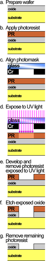
Lithography uses beams of light, ions, or electrons to create patterns on a silicon wafer. The process involves several steps. Before a complex nanoscale pattern can be fabricated, a wafer is typically coated with a soft, thin layer of light-sensitive or electron-sensitive material known as a resist.
The NanoFab’s automated liquid resist coater applies coatings by either spraying the material on a wafer or placing a droplet at the center of a wafer that is spun at high speed. The rapid rotation ensures that the liquid spreads uniformly across the sample. The NanoFab also has a suite of manual spin coaters.
Once the wafer has been coated with a light-sensitive resist, an opaque mask with transparent areas that trace out a specific pattern may be placed either directly on the resist-coated wafer or at a distance above it. The mask allows an overhead light source to shine through and strike the resist only in that specific pattern. The light beam chemically alters the regions of the resist it strikes, either strengthening or weaking the chemical bonds, depending on the resist’s composition.
If the light strengthens the bonds, an example of a negative resist, those regions will remain intact even after a liquid developer dissolves the rest of the resist-coated surface. This creates a raised pattern on the wafer. Conversely, a weakened coating, known as a positive resist, is more susceptible to the developer, so it will dissolve away, leaving the rest of the coating intact. This creates a depressed pattern on the wafer.
Users can choose among several lithographic tools available at the NanoFab. A laser pattern generator employs a laser to directly write patterns onto a wafer or a blank thin film to create a photomask. Two contact aligners at the NanoFab, the Heidelberg MLA150 and the Suss MicroTec MA6/BA6, enable researchers to precisely align several different photomasks on a wafer in order to create a complex, precise pattern.
Other lithography instruments also use photomasks but don’t require direct contact with a wafer. Known as steppers, these tools automatically load cassettes of wafers into a chamber containing an intense light source. The light shines through a photomask and is then projected by a lens onto individual wafers coated with a photoresist. The steppers can process up to 84 wafers in just one hour.
The NanoFab’s two direct-write electron beam lithography instruments employ a scanning beam of electrons to draw customized patterns on a wafer coated with an electron-sensitive resist film. Electron beam lithography offers the advantage of writing on both flat and curved surfaces.
In contrast, the NanoFab’s two focused ion beam (FIB) instruments directly chisel out material from a wafer to create a pattern, without the need for a resist coating.
Before they undergo further processing, wafers must be cleaned. To protect researchers from exposure to the harsh chemicals necessary for cleaning, the compounds are applied in one of the NanoFab’s three enclosed airtight automated systems.
Etching
Lithographed wafers must undergo etching—the process of selectively removing material—in order to reveal the pattern that beams of electrons or photons have imprinted. The NanoFab provides tools for both dry and wet etching. In a wet etch, the entire wafer is immersed in a solution that dissolves a specific material. The challenge is to remove only that material—for instance a thin gold film sitting atop a glass slide—and to leave the underlying glass in pristine condition.
Dry etching uses gases to remove coatings and is performed under vacuum. Each of the NanoFab’s 18 instruments for dry etching tightly control both the flow of gas and the pressure in the vacuum chamber.

Deposition
After fabricating a pattern on a wafer, researchers may wish to deposit additional layers of material on the chip. One method of applying a uniform layer, known as sputtering, uses an ion beam to bombard a solid target. Acting like a miniature sand blaster, the beam sputters, or ejects, material from the target in the form of an ionized gas. An electric field then directs the gas to condense onto and uniformly coat a wafer.
The NanoFab employs several sputtering tools, One of the newest instruments automatically loads and unloads wafers into two chambers, each of which contains six different solid targets. The fully automated instrument can stack multiple layers of material on a wafer, with researchers choosing the composition of each layer from among the 12 targets.
Nanocharacterization
Once completed, a device or thin film must be inspected to determine how well it meets the specified design. The NanoFab has an entire bay devoted to measuring the thickness, strength, optical properties, and surface features of materials.
Two contact profilometers, the Bruker Dektak XT and the Bruker Dektak 6M, use a small stylus that rides over the surface of a wafer in order to measure the varying thickness of an applied thin film. The instruments can detect changes in depth ranging from 1 millimeter (mm) down to 5 nanometers (nm). A third, non-contact profilometer uses light instead of a stylus to measure tiny variations in height and roughness across a surface.
The NanoFab’s stress measurement tool uses a laser interferometer to measure the curvature of a wafer before and after a thin film is deposited on its surface. By comparing the two curvatures, the instrument calculates the extent to which the thin film has ever so slightly bowed the wafer, a measure of stress.
The laboratory’s optical microscopes, which include the Nikon L200 compound microscope and two stereo microscopes, the Olympus SZH10 and the Nikon SMZ1500, use both reflected and transmitted light to inspect thin films and samples. Collectively, the microscopes magnify features from 7 to 1,000 times their original size. Each instrument features an integrated five-megapixel camera that captures high-resolution digital images of substrates ranging from wafers 150 mm (about six inches) in diameter down to pieces as small as 1 mm.
The NanoFab’s ellipsometer measures changes in the polarization of hundreds of wavelengths of light, ranging from the infrared to deep ultraviolet, when they are either reflected from or transmitted by the surface of a wafer. These changes primarily reveal the thickness of a thin film deposited on the wafer but also provide a measure of the optical properties, surface roughness, composition, concentration of dopants, and crystalline structure of the film.
Finally, the laboratory’s five electron microscopes, which include two field emission scanning electron microscopes and two dual beam scanning electron microscopes provide detailed topographic maps of thin films or substrates. The NanoFab’s transmission electron microscope can detect variations in thick ness only a few atoms in diameter.