
Official websites use .gov
A .gov website belongs to an official government organization in the United States.
Secure .gov websites use HTTPS
A lock (
) or https:// means you’ve safely connected to the .gov website. Share sensitive information only on official, secure websites.
NanoFab Tool: J. A. Woollam M-2000 DI Spectroscopic Ellipsometer
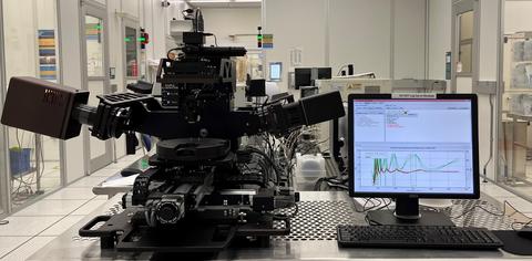
J. A. Woollam M-2000 DI Spectroscopic Ellipsometer
The J. A. Woollam M-2000 DI spectroscopic ellipsometer provides fast and accurate thin film characterization over a wide spectroscopic range. The high speed CCD detector automatically collects data at hundreds of wavelengths ranging from infrared to deep ultraviolet at multiple angles. The user-friendly modeling software can analyze the collected data to characterize film thicknesses, indices of refraction, and extinction coefficients on single layer or multilayer film stacks.
Specifications/Capabilities
- Automated X-Y sample translation.
- Automated tip and tilt alignment.
- Automated sample height alignment.
- Automated angle adjustment ranging from 45° to 90°.
- Wavelength range: 193 nm to 1690 nm.
- Minimum measurement beam diameter: 300 µm using focusing probes.
- High speed charge-coupled device (CCD) detector.
- Integrated camera for viewing the measurement light beam's location.
- User friendly software for data acquisition and data analysis.
Usage Information
Supported Sample Sizes
- Maximum wafer diameter: 200 mm (8 in).
- Small pieces supported: Yes.
- Maximum thickness: 5 mm.
Typical Applications
- Characterization of thin films.
- Measurement of thickness and optical constants on single or multilayer stack.
- Characterization of oxides, photoresists, nitrides, polymers, metals, and other thin films.
- Mapping of film uniformity.
- Determination of deposition rates, etch rates, and total film growth.