
Official websites use .gov
A .gov website belongs to an official government organization in the United States.
Secure .gov websites use HTTPS
A lock (
) or https:// means you’ve safely connected to the .gov website. Share sensitive information only on official, secure websites.
NanoFab Tool: Sensofar Optical Profilometer
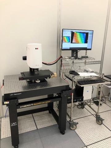
Photo of the Sensofar optical profilometer
Credit:
NIST
The Sensofar optical profilometer is used to measure height variations including step heights and roughness across a surface using light. It uses a nondestructive and non-contact surface metrology technique which can measure relatively large areas in a short amount of time.
Specifications/Capabilities
- Vertical measurement resolutions down to 1 nm
- Lateral resolution down to 50 nm
- Microscope vertical axis travel of 40 mm
- 1360 x 1024 pixel measurement array
- 200 mm x 200 mm stage travel
- Ability to stitch scans across large areas
- Simple, easy to use joystick operation
Typical Applications
- Profiling semiconductor device structures
- Measuring large area arrays
- Imaging MEMs structures
- General topographic materials imaging
Created April 10, 2019, Updated March 4, 2025