
Official websites use .gov
A .gov website belongs to an official government organization in the United States.
Secure .gov websites use HTTPS
A lock (
) or https:// means you’ve safely connected to the .gov website. Share sensitive information only on official, secure websites.
NanoFab Tool: Heidelberg Instruments DWL 2000 Laser Pattern Generator
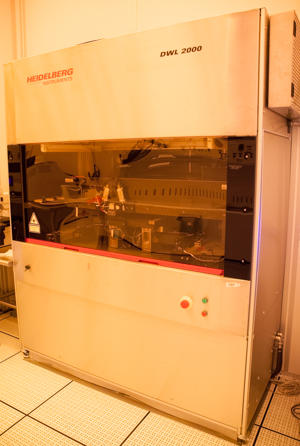
The Heidelberg Instruments DWL 2000 Laser Pattern Generator uses a high resolution laser to expose photoresist with features as small as 700 nm. This system is primarily used for patterning chrome on glass photomasks. The laser writer can process masks up to 6 inch squares. Standard processes include photomask patterning for use in both contact and stepper lithography.
Specifications/Capabilities
- Laser wavelength: 405 nm.
- Minimum feature size: 700 nm.
- Write speed: 110 mm2 / min.
- Address grid: 20 nm.
- Patterning to substrate edge with optical autofocus.
- Allowed data formats: DXF, GDS-II, CIF, and Gerber.
- Alignment system for exposing patterns on existing structures.
- Closed loop environment system.
Usage Information
Supported Sample Sizes
- Standard quartz 5 inch 120 mils thick photomasks
- Standard quartz 6 inch 120 mil thick photomasks (6025 plates)
- Standard quartz 6 inch 250 mil thick photomasks (6025 plates)
Typical Applications
- Micrometer and sub-micrometer lithography.
- Photomask patterning for:
- Contact lithography.
- Stepper lithography.