
Official websites use .gov
A .gov website belongs to an official government organization in the United States.
Secure .gov websites use HTTPS
A lock (
) or https:// means you’ve safely connected to the .gov website. Share sensitive information only on official, secure websites.
NanoFab Tool: Toho Technology FLX-2320 Stress Measurement Tool
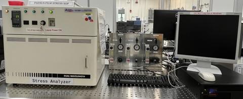
Toho Technology FLX-2320 Stress Measurement Tool
The Toho Technology FLX-2320 stress measurement tool uses a laser interferometer to measure the curvature of a wafer before and after film deposition. It then compares the two measured curvatures to calculate the stress on the deposited film. The Toho quickly performs measurements at user selectable orientations and temperatures and can be used for two dimensional stress mapping on wafers ranging from 200 mm diameter down to 75 mm diameter.
Specifications/Capabilities
- Substrate temperature range: Room temperature to 500 °C.
- Stress Range: 1 MPa to 4 GPa.
- Scan rate: 6 seconds per scan.
- Repeatability: 1 MPa.
- Resolution: 1 MPa.
- Two-dimensional mapping of stress.
Usage Information
Supported Sample Sizes
- Maximum wafer diameter: 200 mm (8 in).
- Small pieces supported: No.
- Wafer diameters: 200 mm (8 in), 150 mm (6 in), 100 mm (4 in), and 75 mm (3 in).
- Maximum thickness: 1 mm.
Typical Applications
- Measurement of film stress.
- Stress characterization of membranes.
- Minimization of stress in multilayer thin films.
- Measurement of stress as a function of temperature.
- Stress mapping.
- Characterization of wafer curvature.