
Official websites use .gov
A .gov website belongs to an official government organization in the United States.
Secure .gov websites use HTTPS
A lock (
) or https:// means you’ve safely connected to the .gov website. Share sensitive information only on official, secure websites.
NanoFab Tool: Suss MicroTec ACS200 Automated Resist Coater
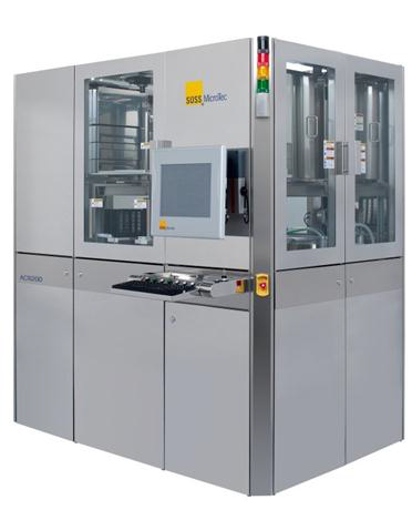
The Suss MicroTec ACS200 is an automated photoresist coating and baking station with cassette-to-cassette substrate operation. It supports both spin coating and spray coating of photoresist on a variety of substrates. The tool provides complete resist coating capabilities, including hotplate baking up to 250 °C and automated edge-bead removal with backside rinse.
Specifications/Capabilities
- Gyrset spin coat & Alta spray coat modules.
- 250 °C programmable hotplate.
- Automated edge-bead removal and back side rinse.
Usage Information
Supported Sample Sizes
- Maximum wafer diameter: 200 mm (8 in).
- Small pieces supported: Yes.
- Maximum substrate thickness: 5 mm.
- Wafer diameters supported:
- 50 mm (2 in).
- 75 mm (3 in).
- 100 mm (4 in).
- 150 mm (6 in).
- 200 mm (8 in).
- Photomask sizes supported:
- 125 mm x 125 mm.
- 150 mm x 150 mm.
Typical Applications
- Photoresist coating for optical pattern exposure.
- Photoresist coating for mask production.