
Official websites use .gov
A .gov website belongs to an official government organization in the United States.
Secure .gov websites use HTTPS
A lock (
) or https:// means you’ve safely connected to the .gov website. Share sensitive information only on official, secure websites.
NanoFab Tool: Heidelberg MLA150 Maskless Aligner
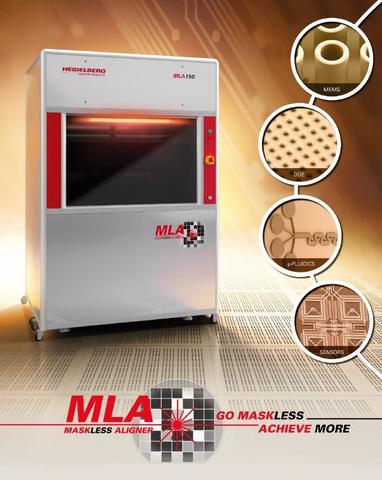
The MLA150 has been specifically designed for direct-wafer writing and easy operation. It offers all the capabilities that are required for single layer and multi-layer photolithography and even overcomes some of the limitations of photomask based exposure technologies because MLA150 exposure is non-contact approach. What set MLA150 apart from mask writer are the fast exposure speed, dual laser wavelengths and convenient alignment system. Alignment in multi-layer applications can be achieved automatically by using three integrated cameras with varying resolution while manual alignment is still available as needed.
Specifications/Capabilities
- Minimum feature size: 1 µm
- Overlay accuracy (front): 500 nm
- Overlay accuracy (back): 1000 nm
- Maximum exposure area: 150 x 150 mm2
- Exposure speed: 10-15 mins for 100 x 100 mm2
- Light source: diode lasers, 8W at 405 nm and 2.8 W at 375 nm.
- Substrate size: 6 x 6 mm2 to 200 x 200 mm2
- Maximum substrate thickness: 6.3 mm
- Size detection: automatic
- Alignment mode: front-size and back-size; automatic and manual
Typical Applications
- Medical devices.
- Biofluidic devices.
- Microelectromechanical systems.
- Thermal sensors.
- Printing micrometer size and larger features.