U.S. flag

An official website of the United States government

Official websites use .gov
A .gov website belongs to an official government organization in the United States.

Secure .gov websites use HTTPS
A lock ( ) or https:// means you’ve safely connected to the .gov website. Share sensitive information only on official, secure websites.

Projects/Programs

Displaying 76 - 100 of 149

Integrated Testbeds for Advanced Metrology

Ongoing
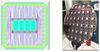
Crossbar Memory Arrays An especially prolific structure in memory architectures aimed at accelerating neural network operation is the crossbar array (Fig. 1). We produce medium-scale arrays that hold up to 20,000 nanodevices which can be characterized, read from, and written to individually or in...

Kinetic Inductance Spectrophotometry

Ongoing
The Kinetic Inductance Spectrophotometry Project is developing novel superconducting detector and readout technologies targeting next generation large-scale hyperspectral imaging applications. Within this application space, the transition-edge sensor (TES) microcalorimeter is the most mature...

Laser-wavelength conversion with nonlinear photonics

Ongoing
Many sophisticated technologies, including detection and characterization of biological samples, quantum sensing of magnetic and electric fields, time standards based on atomic clocks, and precision metrology, demand versatile laser sources spanning a broad range of wavelengths. Nonlinear optics...

Lead-Free Surface Finishes for Electronic Components: Tin Whisker Growth

Completed
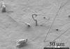
Tin is widely used as a coating in the electronics industry because it provides excellent solderability, ductility, electrical conductivity, and corrosion resistance. Unfortunately, tin whiskers often grow spontaneously from pure tin electrodeposits and short-circuit finely pitched electrical...

Long Wavelength Sensors and Applications

Ongoing
Our project designs and micro-fabricates custom devices that achieve sensitivity at fundamental limits and are based on the principles of superconductivity. We often work in large collaborations to apply these devices to challenging measurements of high scientific interest, such as those which...

Low Temperature Regenerator and Pulse Tube Losses

Ongoing
All-digital radio communication between the various forces of the U.S. military is required to improve communications to the level needed in the near future. Such communication requires analog-to-digital converters of speeds only possible with low temperature superconducting electronics. The...

Magnetic Imaging

Completed
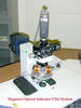
Advanced magnetic devices and storage media will rely on ultra thin ferromagnetic films; since such films are quasi two-dimensional magnets, they can have strong perpendicular magnetic anisotropy (PMA). Optimization of future materials, including improved yields, requires an ability to measure film...

Magnetic Nanostructures for post-CMOS Electronics

Completed
We focus primarily on arrays of magnetic nanostructures in order to reveal how defects alter the fundamental physics of magnetization reversal processes in the nanometer regime. We have an integrated approach that consists of four inter-related elements. The first element, film edge metrology...

Magnetic Random Access Memory

Ongoing
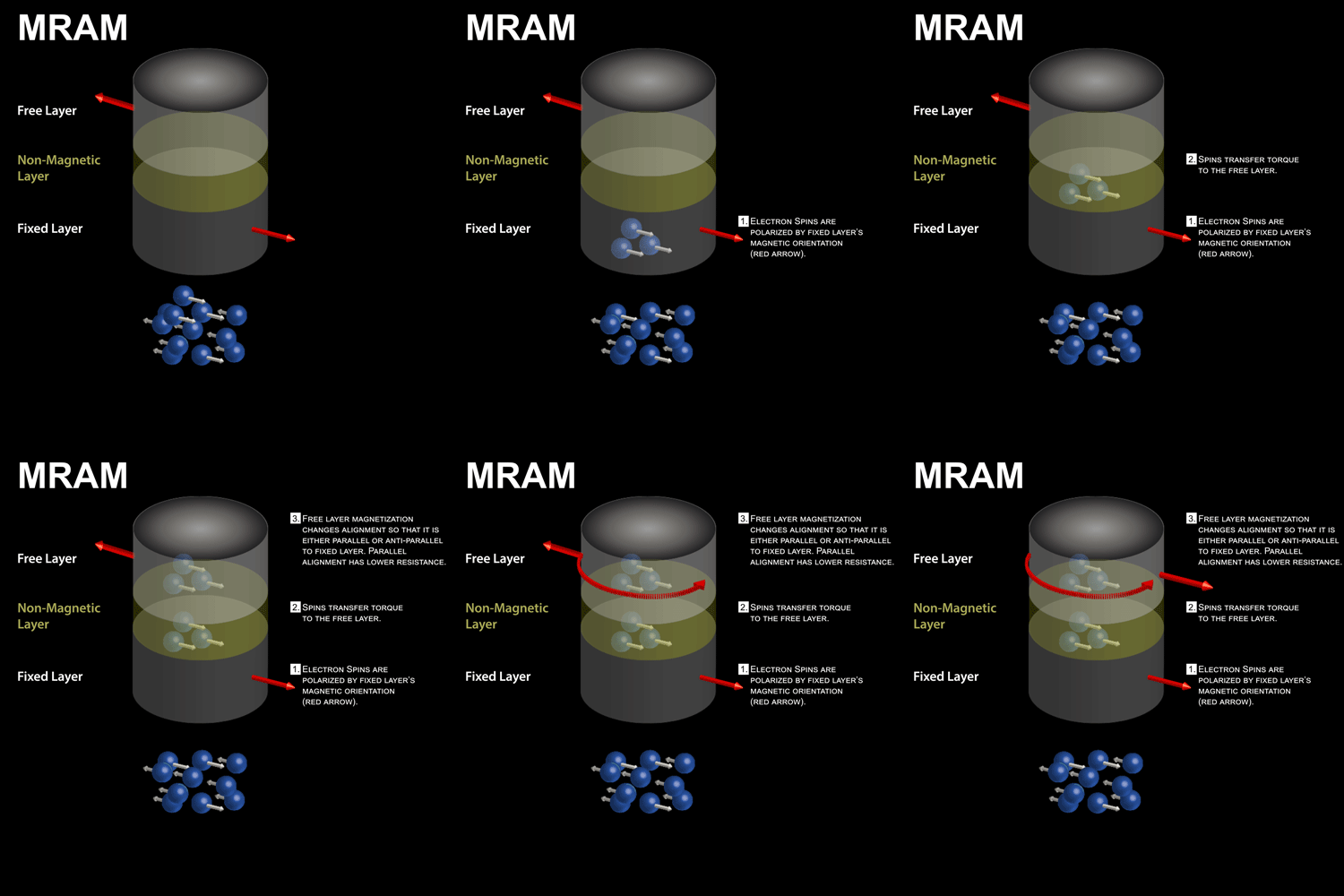
Focus areas include (1) the fundamental understanding of the interactions between spin and magnetic materials and materials with large spin-orbit scattering; (2) the nonlinear dynamics of both individual and interacting nanoscale magnetic systems; and (3) the role of thermal noise in nanomagnetic...

METIS

Ongoing
A Metrology Exchange to Innovate in Semiconductors

Metrology for extreme ultraviolet lithography

Ongoing
Patterning with light 13 nm brings a host a new challenges Light at 13 nm is well within the vacuum ultraviolet, where radiation is strongly absorbed by all materials. This requires that the technology take place in vacuum and rely on mirrors rather than lenses. Moreover generating sufficient...

RF Metrology for High-Frequency Transistor Models

Ongoing
Due to the challenges of high-frequency measurements, that includes inaccuracy in on-wafer calibration and a lack of instrumentation for transistor characterization, models are currently extracted from low frequency measurements and extrapolated to higher frequencies. This methodology has been shown...

Metrology for Integration of New Magnetic Materials

Ongoing
Integration of magnetic materials remains a key challenge facing advanced packaging technologies. High power applications require voltage conversion at or near the die, and most practical power converters rely on inductors. Beyond power electronics, integration of magnetic components such as...

Metrology of the Ohm

Ongoing
The Metrology of the Ohm Project has been a leader in providing internationally consistent resistance standards that are readily available to support the scientific and industrial foundations of the U.S. economy. Through this very broad customer base, the activities of the project enable cost...

Metrology of Purity and Contaminants in Solid Materials

Ongoing
Purity evaluations of high-purity bulk materials used in chips manufacturing are calibrated against reference materials that are often not matrix-matched to the materials under test. In other words, differences in the compositions of the calibrants and the samples being analyzed can result in large...

Micro- and Nanoelectromechanical Systems

Completed
MEMS/NEMS are enabling technologies that bring new functionalities with the potential to radically transform markets ranging from consumer products to national defense. The meteoric rise of the smartphone is an excellent example, in which MEMS accelerometers, gyroscopes, microphones, displays, and...

Multiscale Modeling and Validation of Semiconductor Materials and Devices

Ongoing
The limitations of scaling traditional CMOS (complementary metal-oxide semiconductors) designs have necessitated that the semiconductor industry consider new materials and design concepts. For wide bandgap semiconductor devices, optimization of materials and fabrication processes is needed to...

Nanocalorimetry

Completed
The global market for semiconductor chips is $270 billion. Growth in this industry is driven by the need to enhance performance by packing more transistors into the same chip area, with a relationship between feature size and time that approximately follows Moore's Law. As the feature size shrinks...

Nanocalorimetry for Semiconductors and Semiconductor Process Metrology

Ongoing
In September 2022, NIST published a report titled Strategic Opportunities for U.S. Semiconductor Manufacturing , which cited, among other challenges, the need to understand and improve heat dissipation and performance in advanced microelectronics. Specifically, there needs to be better measurements...

Nanoelectromagnetics

Ongoing
The primary goal of this program is metrology that enables advanced nanoscale device (including electronics, spintronics, and life science) development. Based on current trends in electronics, we are focusing on metrology for two classes of devices: (1) nanoscale devices utilizing and exploring new...
Was this page helpful?