
Official websites use .gov
A .gov website belongs to an official government organization in the United States.
Secure .gov websites use HTTPS
A lock (
) or https:// means you’ve safely connected to the .gov website. Share sensitive information only on official, secure websites.
Summary
A comprehensive understanding of how current and next-generation materials impact the performance of semiconductor devices is critical to U.S. Semiconductor Manufacturing.
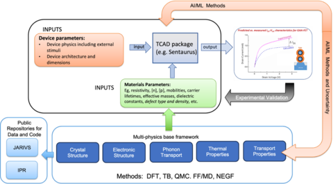
This project will develop qualitative and quantitative models for advanced semiconductor heterostructures, including material properties and the impact of the interface quality via multi-scale, multi-fidelity computational approaches.
Grand Challenge 4: Modeling and Simulating Semiconductor Materials, Devices, and Components
Description
Integrated multi-physics simulation and validation.
The limitations of scaling traditional CMOS (complementary metal-oxide semiconductors) designs have necessitated that the semiconductor industry consider new materials and design concepts. For wide bandgap semiconductor devices, optimization of materials and fabrication processes is needed to improve the device yield and reliability. Future innovations are dependent on developing multi-scale modeling tools and data to predict how new materials and advanced designs will impact device performance.
This project will develop multi-scale models to predict the thermal, chemical and electrical properties of the materials and interfaces, validating these predictions with available experimental measurements, and using machine learning and AI models to both accelerate predictions and facilitate uncertainty quantification.
Multi-scale modeling tools accelerate advanced semiconductor device deployment.
The data and models developed will be integrated with currently available semiconductor software materials property tools and disseminated as open-source code and data. The goal is to enable industrial users to be able to assess how changing a material or interface state will alter the device properties. Designers need to know how replacing a transistor channel, gate, or gate dielectric material will impact the performance and interactions with the rest of the device, as well as how device scaling may impact the defects formed due to reduced dimensions and increased mechanical stresses.
Additional Technical Details
JARVIS: Joint Automated Repository for Various Integrated Simulations, https://jarvis.nist.gov/