
Official websites use .gov
A .gov website belongs to an official government organization in the United States.
Secure .gov websites use HTTPS
A lock (
) or https:// means you’ve safely connected to the .gov website. Share sensitive information only on official, secure websites.
Summary
Advanced methods to measure the thermal properties of thin films and interfaces are required to understand and improve microelectronic device fabrication, performance, heat dissipation and reliability.
This project will build upon nanocalorimeters designed, fabricated, and calibrated at NIST to directly measure transition temperatures, reaction temperatures and specific heat capacity of nanoscale materials and devices for microelectronics, and support other efforts within the CHIPS R&D community.
Grand Challenge 4: Modeling and Simulating Semiconductor Materials, Designs, and Components
Description
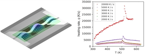
Left: Vibrational mode of the nanocalorimetry sensor membrane to determine sample mass on it. Right: Nanocalorimetry data for the very fast crystallization of a 30 nm layer of an experimental Ag-In-Sb-Te (AIST) memory material.
In September 2022, NIST published a report titled Strategic Opportunities for U.S. Semiconductor Manufacturing, which cited, among other challenges, the need to understand and improve heat dissipation and performance in advanced microelectronics. Specifically, there needs to be better measurements for the thermal behavior of as-fabricated, very small-scale devices, materials and interfaces.
Most of the existing methods, standards, and published databases for thermal properties are either directly or indirectly obtained from measurements on macroscopic bulk materials; this is a source of error and widely known as a major gap in thermal modeling of small devices. In addition to basic device and material thermal properties, thermal reliability of microelectronics is critical and is measured with accelerated thermal cycling for lifetime prediction, which makes it time consuming and expensive, so there is a desire to accelerate this type of testing to collect data more quickly.
Fast thermal cycling method is needed to accelerate the evaluation of stability and lifetime prediction of stacked thin films, interfaces and devices.
This project will develop and apply the nanocalorimetry-based metrology for in situ monitoring of two complex and critical semiconductor fabrication processes - Atomic Layer Deposition and Plasma Processing. Advances in these areas could increase device yield, process control and reproducibility, thereby reducing waste and lowering costs for semiconductor manufacturers.