Summary
Much of the activity of the UV Physics Group is aimed at supporting the R&D effort by the microelectronics industry to develop Extreme Ultraviolet Lithography (EUVL) to pursue the goal set by Moore's Law of doubling the number of transistors on a computer chip every two years. Photolithography is the patterning technology used as the first step of production of microelectronics, and it sets the limits on the transistor size. Currently the lithographic patterns are created using lasers working at 193 nm wavelength. Since the minimum feature size in a pattern is related to the wavelength of light used, and we are close to the smallest feature size efficiently producible with 193 nm light, the semiconductor industry has turned to EUV light at 13 nm to meet the Law's challenge of fitting more transistors on a chip.
Description

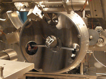
A large EUV optic mounted for reflectometry measurements.
Patterning with light 13 nm brings a host a new challenges Light at 13 nm is well within the vacuum ultraviolet, where radiation is strongly absorbed by all materials. This requires that the technology take place in vacuum and rely on mirrors rather than lenses. Moreover generating sufficient radiation in the EUV is extremely difficult, so all efforts must be taken to ensure that the reflective optics provide the highest throughput for the light. The EUV sources are pulsed at very high repetition rates, requiring new tools to measure their power output. High throughput of the light requires that the mirrors have the highest possible reflectivity and be uniform over the whole surface. The source output characterization issues are being addressed by our radiometry [BL-2] activity; mirror efficiency by our reflectometry [BL-7] programs. A large EUVL optic is shown inside the reflectometer chamber in the figure on the upper right.
Mirror reflectivity must remain high over the period of operation of the lithographic tool. The lithographic process involves exposing the pattern to a photoresist that stores the pattern for further processing. The EUV radiation causes chemical changes in the photoresist which creates volatile compounds that may migrate through the vacuum system and adsorb onto the mirrors. We have also developed new metrology to address this issue. Our resist outgassing facility [BL-1] directly measures the damage potential of EUV photoresists using a witness-sample test. We also have a program that measures and models optics contamination on EUV optics.

