Official websites use .gov
A .gov website belongs to an official government organization in the United States.
Secure .gov websites use HTTPS
A lock (
) or https:// means you’ve safely connected to the .gov website. Share sensitive information only on official, secure websites.
Featured Video
News and Updates

Department of Commerce Announces Finalization of CHIPS Incentives with xLight to Support Next-Generation Light Source for Lithography
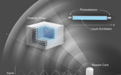
Searching for Sterile Neutrinos

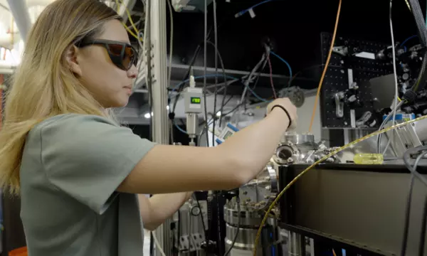
NIST Researchers Probe the Mass of the Electron Neutrino
Blog Posts
Unlocking Our World’s Earliest Secrets — One Tiny Electron at a Time
Why do we exist? It’s a big question — and one that some of NIST’s early universe detectives are getting closer to answering.
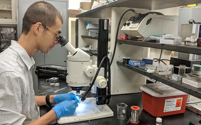
From Pokémon to Physics: My Journey of Perseverance Into Research
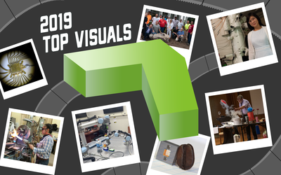
Top 7 NIST Visuals of 2019