
Official websites use .gov
A .gov website belongs to an official government organization in the United States.
Secure .gov websites use HTTPS
A lock (
) or https:// means you’ve safely connected to the .gov website. Share sensitive information only on official, secure websites.
Precision Imaging Facility
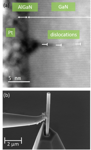
Examples of work in the Precision Imaging Facility. (a) STEM image of a crack (dislocation) formed during growth of an AlGaN shell around a GaN nanowire, and (b) FIB fabrication of an AFM tip with a GaN nanowire contact point.
The Precision Imaging Facility (PIF) is a cooperative research facility at the National Institute of Standards and Technology (NIST) dedicated to the advancement of measurement science through advanced imaging techniques. The facility is located in the Katharine Blodgett Gebbie building in Boulder, Colorado. With primary funding from the 2009 American Recovery and Reinvestment Act (ARRA), NIST acquired three state-of-the-art instruments and built a 3,000 Sq. Ft. custom laboratory to house them: an aberration corrected transmission electron microscope (TEM), a combination focused ion beam/scanning electron beam microscope (FIB/SEM), and a local electrode atom probe (LEAP). The facility continues to grow and evolve as it supports NIST's mission and meets the imaging needs of NIST's world-class researchers.
The Precision Imaging Facility provides the ability to manipulate and characterize matter from the microscopic level down to the atomic scale. As a shared microscopy and microanalysis resource for the NIST Boulder site, the PIF has had a direct impact upon a broad spectrum of successful projects including optimization of superconducting Josephson voltage arrays, fabrication of advanced quantum sensors, measurement of nanowire-based probes and devices, characterization of chip-scale atomic clocks, fabrication of nanoscale magnetic devices, and microscopic investigation of laser-welded metals. These programs rely on the complicated interworking of nanoscale materials and microfabrication technology that can only be probed by advanced imaging tools. For example, the dual beam Focused Ion Beam / Scanning Electron Microscope (FIB/SEM) allows researchers to selectively mill devices and materials in order to reveal internal structure, including subsurface interfaces and defects. The dual beam tool also provides state-of-the-art, high-resolution imaging, which has recently enabled NIST to stand up a new standard reference instrument (SRI 6012 Precision Semiconductor Nanostructures) and a new calibration service (15510S Dimensional Measurement of Nanostructures, traceable to NIST RM8820).
Furthermore, the FIB an indispensable tool for the preparation of samples for the other analytical techniques such as atom probe tomography and TEM. The TEM opens the door to imaging and compositional analysis with sub-angstrom resolution. High-resolution characterization of crystalline materials is vital for the development of single photon emitters, nanoscale light sources and advanced quantum information circuits. In addition, the aberration-corrected TEM can locally investigate chemical composition and by extension can evaluate advanced crystal growth techniques needed for next-generation device development. The local electrode atom probe reconstructs analytic volumes atom by atom, revealing the local chemical composition of structures with and unprecedented combination of chemical sensitivity and spatial resolution. The atom probe technique offers NIST researchers the opportunity to investigate a wide variety of materials including nanoscale semiconductor devices and multilayer systems. Recently, in a collaborative effort with CAMECA and the Colorado School of Mines, NIST has begun work on pushing the boundaries of three-dimensional, atomic-scale tomography through Extreme Atom Probe Tomography (XAPT). Note that the XAPT research depends on the FIB tool, the TEM, the conventional LEAP tool, as well as the Boulder Microfabrication Facility.
The imaging and characterization capabilities provided by these three instruments, in conjunction with associated sample preparation and inspection capabilities also housed in the PIF, provides a uniquely powerful, shared resource. Operation of the PIF is built upon a model of shared costs and shared responsibilities, extending the model and culture established by the cooperative Boulder microfabrication facility. Users share responsibility for stewardship of the equipment by coordinating maintenance, proactively promoting laboratory safety, training new users, and managing tool access. This enables NIST researchers to push the boundaries of microscopy, developing new instrumentation and techniques while engaging both internal colleagues and external collaborators.