Summary
Electromagnetic (EM) systems use magnetic components such as inductors, isolators, and adaptive filters, but these are currently bulky and difficult to integrate with microelectronic circuitry. This limits the utility of the magnetic components. Reducing the size, weight, and energy dissipation of magnetic components and integrating them onto semiconductor chips and into packaging will enable broader exploitation of magnetic materials and provide new mechanisms for the control and manipulation of EM signals.
This program will develop the metrology, materials, and methods needed to integrate magnetic components with semiconductor materials, thereby reducing the size and improving the functionality of EM systems for communications, radar, and advanced computation.
Grand Challenge 3. Enabling Metrology for Integrating Components in Advanced Packaging
Description

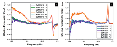
Experimental results for flexible magnetic nanoparticle composite, showing broadband frequency dependence of (a) real, and (b) imaginary parts of the effective complex permittivity.
Integration of magnetic materials remains a key challenge facing advanced packaging technologies.
High power applications require voltage conversion at or near the die, and most practical power converters rely on inductors. Beyond power electronics, integration of magnetic components such as circulators with state-of-the-art semiconductor amplifiers can significantly reduce the size, weight, and power requirements of semiconductor components while boosting performance.
Innovation in advanced packaging for microelectronics requires integration of magnetic materials, but the required metrology to accurately evaluate and model integrated magnetic materials is currently lacking.
To help solve this problem, this project will address three major needs for measurement and modeling of integrated magnetic materials:
- Magnetic materials and measurements for power electronics
- Magnetic materials and measurements for communications electronics
- Modeling integrated magnetic materials and devices

