
Official websites use .gov
A .gov website belongs to an official government organization in the United States.
Secure .gov websites use HTTPS
A lock (
) or https:// means you’ve safely connected to the .gov website. Share sensitive information only on official, secure websites.
Molecular Dynamics Simulation of Heat Transport in Gate-All-Around Transistors
Summary
Heat management in semiconductor devices is a crucial problem currently limiting device performance and essentially all progress involving reduction of device feature dimensions further into the nanoscale. As of today, no systematic effort aimed at managing heat dissipation at the nanoscale exists.
This project will provide a robust understanding of heat dissipation at the nanoscale and will have a significant impact on semiconductor engineering.
Grand Challenge 4: Modeling and Simulating Semiconductor Materials, Designs, and Components
Description
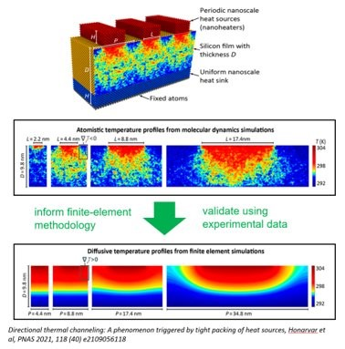
Directly simulate nanoscale heat transport to inform finite element methods Theory will be validated by other CHIPS Metrology funded projects.
Thermal efficiency of semiconductor devices is pivotal to their operation and performance, especially now that the dimensions of transistor features are rapidly shrinking to the nanoscale. A significant knowledge gap persists in accurately describing and quantifying heat dissipation at such scales. Currently, any progress in heat management is achieved through trial and error, as opposed to engineering based on accurate predictions of thermal properties at the nanoscale.
The lack of reliable models capable of describing heat transport at the nanoscale will become even more critical in the next few years, as gate-all-around field-effect transistors (GAAFETs) are poised to replace the existing field effect transistor (FET) technology. One of the major challenges with GAAFETs is the requirement to manage highly localized heat, because the proposed transistor source substructures are essentially nanoscale arrays of nanowires or nanosheets buried inside the gate.
The results of this project will shift the paradigm of nanoscale heat management from trial-and-error to knowledge-based engineering.
This project will use NIST’s computational resources and theoretical expertise to assess heat transport within nanometers of the heat sources created by complementary metal-oxide semiconductors (CMOS) conductive channels. Extensive molecular dynamics simulations will be used to quantify heat transport, including boundary scattering.
Combined with measurements, this project will elucidate the physics behind nanoscale heat transport and provide data toward refining the existing finite-element models and ultimately laying foundation for enhanced transistor-level heat transport in the next-generation semiconductor devices.