
Official websites use .gov
A .gov website belongs to an official government organization in the United States.
Secure .gov websites use HTTPS
A lock (
) or https:// means you’ve safely connected to the .gov website. Share sensitive information only on official, secure websites.
Summary
Advanced bonding and integration physically bring together components, devices, and materials that are produced separately. There are strong economic and functionality incentives to use this approach at a range of physical sizes. Surface bonding efficiency depends on precise surface pre-treatments.
This project will apply unique analytical and metrological capabilities to develop a scientific understanding of bonding processes. This general understanding may provide a predictive framework for rapid known good process (KGP) development which directly impacts chiplet manufacturing.
Grand Challenge 3. Enabling Metrology for Integrating Components in Advanced Packaging
Description
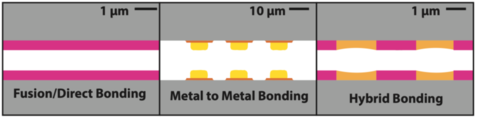
Wide range of bonding applications
The most important part of any bonding process is getting the surfaces to stick. While the physical properties of the films, surfaces, and interfaces in conjunction with the bonding process parameters (pressure, duration, temperature, and post bond anneal) all play important roles, altering the surface physical properties with pre-treatments has been found crucial for consistently achieving a high-quality bond.
However, exactly how such pretreatment methods work is not well understood. Currently, a Known Good Process (KGP) is developed by trial and error, which is inefficient and leaves up to chance the manufacturing advantage that U.S. industry has in Advanced Packaging and Integration.
This work offers the potential for the CHIPS R&D program to strengthen the U.S. position in the field of bonding processes in advanced packaging.
This project will develop surface characterization metrology methods capable of better predicting bond quality based on pre-bonding measurements of surfaces subjected to surface treatments. Such processes are necessary for complex integration of sophisticated components and novel materials for advanced microelectronics packaging.
Bonding processes are broadly utilized by industry. As such, it is difficult to overstate the potential impacts and benefits. Disparate portions of industry are unlikely to come together on their own to solve these problems from a unified cross-application standpoint or fundamental and open point of view.