Official websites use .gov
A .gov website belongs to an official government organization in the United States.
Secure .gov websites use HTTPS
A lock (
) or https:// means you’ve safely connected to the .gov website. Share sensitive information only on official, secure websites.
Research & Development Programs
The purpose of the CHIPS Research and Development (R&D) programs is to advance the development of semiconductor technologies and to enhance the competitiveness of the U.S. semiconductor industry. The CHIPS R&D programs have three goals:
- To establish the capacity to invent, develop, prototype, and deploy the foundational semiconductor technologies of the future – here in America;
- To accelerate ideas to market. We want the best ideas to achieve commercial scale as quickly and cost effectively as possible; and
- To contribute to a robust semiconductor workforce. We want enough inventors, designers, researchers, developers, engineers, technicians, and staff to meet the needs of government and commercial sectors.
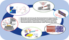
To address these semiconductor R&D ecosystem gaps, CHIPS R&D invests $11 billion under the advanced microelectronics research and development authorities, all of which include some aspect of workforce training. These authorities inform CHIPS R&D programs, which are intended to share infrastructure, participants, and projects. They operate in coordination with the CHIPS Incentives Program, and with microelectronics R&D programs supported by other U.S. federal agencies. CHIPS R&D will be informed by industry’s needs, and innovations from the R&D funding opportunities that will accelerate innovation and increase competitiveness in the American semiconductor industry and establish our leadership in the sector for decades to come.

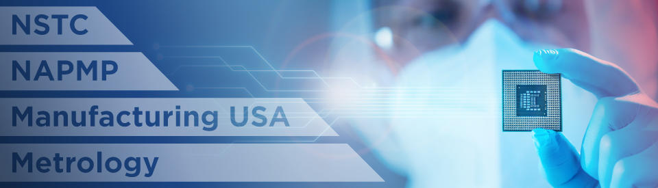
- National Semiconductor Technology Center – A public-private consortium that will serve as the focal point for semiconductor research for the nation.
- CHIPS National Advanced Packaging Manufacturing Program – The U.S. needs to develop the capability to package chips together in multiple dimensions with a variety of functions — known as advanced packaging — to regain and maintain leadership in semiconductor manufacturing.
- CHIPS Manufacturing USA Institute – CHIPS for America established a new Manufacturing USA institute, known as SMART USA (Semiconductor Manufacturing and Advanced Research with Twins USA), dedicated to digital twin technology for semiconductor manufacturing technologies and related workforce training. Learn more about the institute.
- CHIPS Metrology – NIST will conduct the measurement science, or metrology, critical to the development of new materials, packaging, and production methods for semiconductors. NIST will also work on reference materials, reference data, and calibrations for the precision equipment used in chip manufacturing, and advise on the development of standards for processes and cybersecurity.
The Industrial Advisory Committee provides advice to the Secretary of Commerce through NIST on matters relating to microelectronics research, development, manufacturing, and policy — including assessment of the research and development programs that make up the CHIPS for America R&D Office.