
Official websites use .gov
A .gov website belongs to an official government organization in the United States.
Secure .gov websites use HTTPS
A lock (
) or https:// means you’ve safely connected to the .gov website. Share sensitive information only on official, secure websites.
Summary
Advanced packaging involves increasingly challenging requirements for heterogeneous integration and chiplet packaging. Needs such as fine pitch interconnects (<10 μm pitch), finer lines/spaces, and an increasing number of distribution layers will require intensive engineering design to minimize warpage and maximize thermal performance while retaining or improving reliability in harsh conditions over the long-term life of the package. To be successful, research advances must address the most challenging materials and interfaces in the package, such as underfill materials, organic substrates, and molding and potting epoxies. Accurate material property measurements as a function of processing conditions, such as cure time, temperature, and pressure, are critical to inform the predictive models used to analyze how process tool requirements affect the warpage of integrated assemblies and packages. These critical properties must also be known as function of the harsh thermal and environmental conditions that chip packages are exposed to during their service.
The outputs of this project include quantitative measurement methods, open-source materials data, model calibration frameworks, and predictive modeling tools to inform engineering design of advanced packaging systems in practice. These will be socialized with the semiconductor industry to drive polymer materials design and package design improvements required for 3D heterogeneous integration and to maintain standards modernity.
Grand Challenge 3. Enabling Metrology for Integrating Components in Advanced Packaging
Description
Industry needs improved metrology tools to quantify properties of polymeric packaging materials, investigate device-relevant conditions, and ensure quality and reliability.
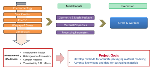
The metrology challenges impacting the U.S. semiconductor industry are at a critical stage and urgently need to be addressed. Currently, most of the polymeric materials for organic laminates, underfills, epoxy molding compounds, build-up films, and adhesives are purchased overseas. The ability to measure, monitor, predict, and ensure quality and reliability in advanced packaging for highly complex, integrated semiconductor manufacturing is a challenge for domestic manufacturers. They are not able to readily obtain the materials data needed to engineer their process flows or verify the thermomechanical properties of their incoming feed materials. Furthermore, many of the present metrological techniques rely on assumptions and simplifications that are increasingly insufficient in the complicated environments, which include fluctuations in temperature and relative humidity, in which packaging materials are deployed. This compromises the validity of the measurements and predictions. Our goal is to develop advanced metrologies, methodologies, and database tools to characterize, test, model, predict, and validate the structure-processing-property relationships of polymeric materials and material interfaces for heterogeneous integration in semiconductor packaging.
The objective of this program is to provide the semiconductor industry with measurement capabilities, knowledge, and open-source data for polymeric materials that are used in next-generation packaging technologies. The measurements and metrological techniques will be valuable tools to help the industry improve the performance of their packaging materials by
- Establishing quantitative structure–property–processing relationships using research grade test materials,
- Accelerating introduction of new and improved packaging materials into process workflow, and
- Developing more accurate predictive mechanical models for advanced packages.
The advancements in thermal analysis, warpage and stress measurement, and modeling will significantly enhance the industry's ability to design and package next-generation electronic devices using advanced materials. We will provide the semiconductor industry with the tools and data to assess the properties of incoming feed stocks and establish uniform test methods. This will address process and device relevant conditions that chip packages are expected to operate. Building on this effort, the research grade materials and test methods developed are intended to serve as platforms to identify opportunities to reduce process qualification times and enable multi-sourced procurements.
Additional Technical Details
This research addresses the challenges the industry is facing in improving the thermo-mechanical performance of advanced packages by developing new methodologies and metrologies for packaging material characterization and predictive modeling. The team will specifically target metrology for packaging optimization. This includes thermal analysis for cure kinetics, coefficient of thermal expansion, mechanical properties, and residual stress measurements in parallel with optical techniques to measure areal warpage and stress distributions. Within a harmonized, collaborative approach the fundamental data and knowledge generated will be directly correlated with materials behavior in a packaging environment. We will relate properties to performance, giving materials suppliers the feedback that they need to develop new materials. Data will be suitable for integration into multi-physics finite element-based modeling (FEM) packages that are used to predict the performance of the entire package under application conditions.