An official website of the United States government
Here’s how you know
Official websites use .gov
A .gov website belongs to an official government organization in the United States.
Secure .gov websites use HTTPS
A lock (
) or https:// means you’ve safely connected to the .gov website. Share sensitive information only on official, secure websites.
The terms “semiconductor” and “chips” refer to an electronic device or system. They are found in household items, such as coffee makers, garage door openers, and refrigerators, as well as in more complex products such as mobile phones, pacemakers, and automobiles. They are crucial to the operation of communication and navigation systems and are key to the technologies of the future, including artificial intelligence and 5G.
Semiconductor Manufacturing Process
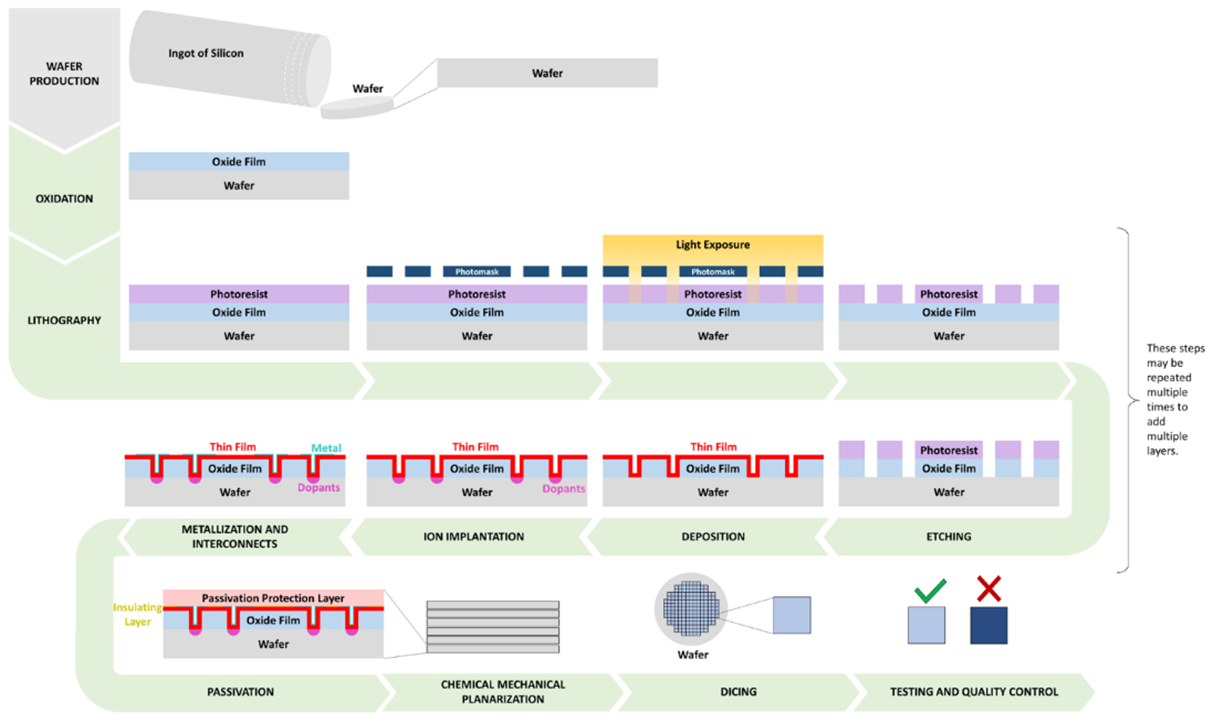
Creating a semiconductor chip involves thousands of steps, and it can take more than 90 days from design to production. The diagram below details the essential steps in the typical manufacturing process using standard silicon wafers.
The semiconductor manufacturing process has several environmental impacts, including energy consumption, water usage, and chemical waste management. The CHIPS Environmental Division works to identify and minimize these impacts through the facilitation of regulatory compliance, risk assessment, and mitigation strategies.
By adhering to environmental laws and proactively engaging early in the application process, we aim to support reducing the impacts of the semiconductor industry and finding a balance between technological advancement and environmental stewardship.
The following steps are essential parts to the typical manufacturing process using standard silicon wafers. To learn more about each step, click on the diagram.
Once the wafer is transported to a fab, the semiconductor fabrication process continues. The following steps are an essential part of the typical “front-end” chip manufacturing process using a standard silicon wafer:
After cleaning, the wafer is placed in a high temperature environment, where pure oxygen and/or water vapor is used to form a thin protective film of silicon dioxide on the wafer and impurities and pollutants are removed. Dry or wet oxidation methods can be used.
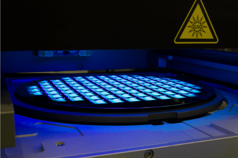
The wafer is covered with a light-sensitive coating called photoresist. The coated wafer is inserted into a lithography machine, where it is exposed to deep UV (DUV) or extreme UV (EUV) light. Light is projected onto the wafer through a transparent plate containing a circuit pattern, known as a photomask, to transfer the desired pattern to the chip.
The wafer is baked and developed, and some of the photoresist is washed away to reveal a three-dimensional pattern of open channels. Etching is then performed in places where the photoresist has dissolved to transfer the circuit pattern permanently onto the wafer. “Dry” or “wet” etching methods can be used; dry methods use gases to expose the pattern, whereas wet methods use chemical baths
Deposition is the process of adding thin layers of material onto the wafer’s surface. The process creates metal (conducting) layers, dielectric (insulating) layers, or semiconducting material layers - depending on the type of structure being made
Once patterns are etched, the wafer is bombarded with positive or negative ions (such as arsenic or phosphorous). These embedded impurities, called dopants, give different parts of the wafer different levels of conductivity to make functional transistors in chips.
Metal layers are deposited onto the wafer’s surface to serve as electrical connections between the various components of the device. These metal layers can be deposited using a variety of techniques. The metal layers are then patterned and etched to form the desired interconnect structures.
Passivation involves the deposition of a protective layer onto the wafer’s surface. This layer serves to protect the delicate underlying structures from damage and contamination during the packaging process and subsequent use. Common passivation offers good adhesion, low moisture permeability, and compatibility with underlying semiconductor materials.
Once one layer is complete, it is flattened and the process is repeated to add a new layer; as a result, at the end of the overall manufacturing process, a single chip may contain dozens of layers.
The wafer, which contains dozens of chips in a grid pattern, is sliced into individual chips to remove the chips from the wafer.