
Official websites use .gov
A .gov website belongs to an official government organization in the United States.
Secure .gov websites use HTTPS
A lock (
) or https:// means you’ve safely connected to the .gov website. Share sensitive information only on official, secure websites.
Nanoscale Device Characterization Division
The Nanoscale Device Characterization Division (NDCD) transforms nano- and atom-scale technologies by advancing measurement science and fundamental knowledge.

The Nanoscale Device Characterization Division (NDCD) is based in Gaithersburg, Maryland, and operates within the Physical Measurement Laboratory at NIST.
The Division's mission is to develop and advance the measurement and knowledge infrastructure to characterize nano- and atom-scale engineered materials and solid-state devices for innovation in information processing, sensing, and future quantum technologies.
The NDCD’s technical activities span atom scale devices, nanoscale spectroscopy, nanoscale imaging, nanoscale processes and measurements, and alternative computing.
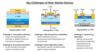
Focus Areas
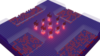
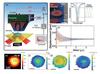
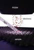
WORLD CLASS ELECTRICAL AND OPTICAL MICROSCOPY provides “local” measurements that characterize nanoengineered solid-state materials and devices as a function of temperature, electrical bias, optical stimulus, or applied magnetic field to reveal the fundamental physical properties and processes that underpin emergent quantum behavior. Advances in nanoscale microscopy instrumentation complement innovative precision electrical and optical spectroscopic measurements, methodology, and test structure design and fabrication.
ADVANCED DEVICE TECHNOLOGIES support the development of measurements to identify root-cause defects which limit the performance, reliability, and commercial potential of electronics designed to operate in extreme environments. Specifically, there is an emphasis on power devices responsible for conditioning, conversion, and delivery of power within data center environments and a variety of electric transportation applications. There is also a strong emphasis on the development of devices, circuits, and systems which operate in the cryogenic environments necessary to support large-scale (meaningful) quantum computation.
MEASUREMENT PROBLEMS IN ALTERNATIVE COMPUTING, especially neuromorphic computing and AI, are being addressed, especially neuromorphic computing and AI, by investigating new devices for analog and stochastic computing and exploring new architectures and algorithms, both theoretically and in medium-scale integrated prototypes.
This effort focuses on designing, fabricating, and characterizing hybrid circuit test platforms and disseminating them to researchers in industry and academia to enable more efficient validation of device and circuit properties at increasingly greater complexity and scale.
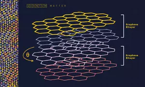
ATOM-SCALE DEVICES develop the foundational knowledge, measurements, and fabrication methods needed to enable nanoengineering of solid-state devices and systems that will lead to new, unexplored emergent quantum behavior.
This effort is pushing electronic and quantum devices and sensors to their fundamental operation limits with single electrons and spins on deterministically placed atoms. These devices will be critical for realizing chip-scale quantum information processing, quantum simulators, and field-deployable quantum electrical standards.
STANDARDS DEVELOPMENT involves engaging in international standards development where rigor in measurement methodology, data analysis, and data reporting facilitate a robust consensus-based standards-creation process.
News and Updates
Projects and Programs
Awards


Press Coverage
Patents
- Hall Effect
The history of the Hall effect begins in 1879 when Edwin H. Hall discovered that a small transverse voltage appeared across a current-carrying thin metal strip in an applied magnetic field. Until that time, electrical measurements provided only the carrier density-mobility product, and the separation of these two important physical quantities had to rely on other difficult measurements. The discovery of the Hall effect enabled a direct measure of the carrier density. The polarity of this transverse Hall voltage proved that it is in fact electrons that are physically moving in an electric current. Development of the technique has since led to a mature and practical tool, which today is used routinely for characterizing the electrical properties and quality of almost all of the semiconductor materials used by industry and in research labs throughout the world.
Contacts
Division Chief
-
(301) 975-2048