
Official websites use .gov
A .gov website belongs to an official government organization in the United States.
Secure .gov websites use HTTPS
A lock (
) or https:// means you’ve safely connected to the .gov website. Share sensitive information only on official, secure websites.
Summary
Specialized imaging methods with high spatial resolution are essential for advancing the physical understanding of emergent materials in advanced electronics and quantum-based devices. Photoemission electron microscope (PEEM) is a full-field imaging technique which can resolve surfaces in real space and momentum space providing rich information of its electronic structure. We will further advance our laboratory-based PEEM with novel photon sources to expand on new measurement modalities such as imaging electron dynamics and electron response to light polarization.
Description
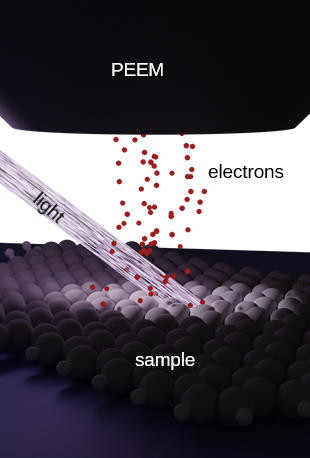
Schematic of a PEEM measurement.
With the rise of emergent material systems, nanoscale devices and components, there is a need to assess their electronic properties at similar length scales. Bulk-sensitive measurements provide characteristic information averaged over the sample or device, and these properties may not be uniform over macroscopic or mesoscopic length scales. There is a need to close the measurement gap between spatially-integrated photoemission techniques and atomically-resolved scanning probe-based techniques to tease out the interplay between microstructure and electronic structure, and how ensemble or collective properties impact novel and quantum materials.
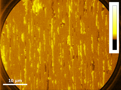
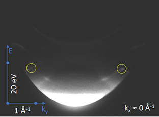
PEEM images are generated by photoelectrons that are ejected from a sample by photons. PEEM is an electron microscope with many contrasting mechanisms due to topography or electronic variation of a sample. Currently, real space imaging can reach a resolution of ~50 nm and can be coupled with energy filtering capability. The PEEM is also capable of μ-angle resolved photoemission (μ-ARPES) for samples with uniformity of ~10 μm with an energy resolution of < 300 meV. Other capabilities include in-situ heating (up to 1500 K) and cooling (~120 K).
Laboratory-based PEEM measurement capability will be advanced by integrating it with laser-based photon sources in 2021. We will gain more measurement modalities -- expanded accessible “information depth,” polarization control and time resolved capability to alter systems from equilibrium. By extending the current PEEM instrument capability to beyond continuous wave plasma-based photon sources – it provides additional capability to tune the “information depth” by altering the kinetic energy of the ejected photoelectrons. This can be an analytical parameter to discern between electronic properties or processes are at the surface or below the surface (i.e., in the bulk or buried interface). The other capabilities gained allows for dynamic or non-linear processes to be investigated which are becoming critical for understanding the microscopic physical processes underpinning the limited progress of new electronic devices and structures. Novel photon sourced coupled to a PEEM allow for us to advance our understanding in the physical processes behind emerging nanotechnologies with high spatial resolution, electronic contrast, and dynamics.
Major Accomplishments
2022
- Integration with high repetition rate, tunable deep UV laser system
2021
2019
- Arrival of NIST PEEM instrument and commissioning of instrument
2017
- Collaboration with Center of Integrated Nanotechnologies (Sandia NL) for initial PEEM experiments (2017-2018)