
Official websites use .gov
A .gov website belongs to an official government organization in the United States.
Secure .gov websites use HTTPS
A lock (
) or https:// means you’ve safely connected to the .gov website. Share sensitive information only on official, secure websites.
Nanoscale Reliability Group
The Nanoscale Reliability Group develops and disseminates science, standards, and technology for high-resolution measurements of material structure, chemistry, and physical properties, to ensure reliability of materials and devices with critical dimensions in the micrometer to nanometer regime.
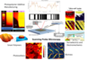
The Nanoscale Reliability Group is part of the Applied Chemicals and Materials Division (ACMD) on the NIST Boulder campus. The group develops innovative metrologies and standards in the realms of electron, ion, optical, X-ray and scanned probe microscopies, to identify and locate atomic, nanoscale and microscale defects, and to determine physical responses of materials. Innovations include novel instruments, unique operating modes, and new analysis methods. The metrologies are deployed in key application areas including semiconductor and advanced manufacturing materials. The group seeks close interaction with external stake holders to ensure technology adoption and maximize impact of our applied programs.
News and Updates
GROUP PATENTS
NIST encourages patent protection on inventions when a patent would further the interests of U.S. manufacturing, increase the potential for current or future commercialization or use of the technology, would likely to lead to a license, would have a positive impact on a new field of science or technology and/or the visibility and vitality of NIST, or would further the goals of collaborative agreements.
Although patents are issued in the name of the inventor, the rights to inventions resulting from government work belong to the government. NIST's Technology Partnerships Office negotiates licensing of patented NIST technology.
Patents:
Sample holder, detector mask, and scope system for analytical transmission scanning electron microscopy
9,970,859; 9,746,415
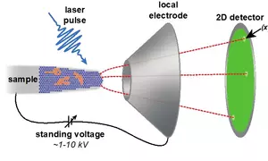
Imaging spectrometer for extreme ultraviolet atom probe tomography
10,153,144; 9,899,197
Electron vibrometer for atomic force microscopy
10,060,946
Provisional/Pending Patents:
Dynamic multi-wavelength and sample voltage atom probe tomograph feedback control system
63/563,030
Additive manufacturing polyelectrolyte resin and additively manufacturing
18/206,667
Making a hydrogel from a sacrificial ionic scaffold
19/058,167
Projects and Programs
Publications
Awards


Press Coverage
Group Staff
Name | Phone | Email | Primary Project(s) |
|---|---|---|---|
| Benjamin Caplins | (303) 497-6703 | benjamin.caplins [at] nist.gov (benjamin[dot]caplins[at]nist[dot]gov) | Extreme Atom Probe Tomography |
| Ann Chiaramonti Debay | (303) 497-5701 | chiaramonti [at] nist.gov (chiaramonti[at]nist[dot]gov) | Extreme Atom Probe Tomography |
| Russell (Colby) Evans | (303) 497-6226 | russell.evans [at] nist.gov (russell[dot]evans[at]nist[dot]gov) | |
| Callie Higgins | (303) 497-5991 | callie.higgins [at] nist.gov (callie[dot]higgins[at]nist[dot]gov) | Photopolymer Additive Manufacturing |
| Jason Holm | (303) 497-4335 | jason.holm [at] nist.gov (jason[dot]holm[at]nist[dot]gov) | |
| Orion Kafka | (303) 497-6597 | orion.kafka [at] nist.gov (orion[dot]kafka[at]nist[dot]gov) | |
| Jason Killgore | (303) 497-4729 | jason.killgore [at] nist.gov (jason[dot]killgore[at]nist[dot]gov) | |
| Thomas Kolibaba | (303) 497-5811 | thomas.kolibaba [at] nist.gov (thomas[dot]kolibaba[at]nist[dot]gov) | |
| Elisabeth Mansfield | (303) 497-6405 | elisabeth.mansfield [at] nist.gov (elisabeth[dot]mansfield[at]nist[dot]gov) | Electronic Material Characterization |
| Rion Wendland | (303) 497-5991 | rion.wendland [at] nist.gov (rion[dot]wendland[at]nist[dot]gov) | Photopolymer Additive Manufacturing |
| Ryan White | (303) 497-3938 | ryan.white [at] nist.gov (ryan[dot]white[at]nist[dot]gov) | Precision Imaging Facility |
Contacts
Group Leader
-
(303) 497-4729