
Official websites use .gov
A .gov website belongs to an official government organization in the United States.
Secure .gov websites use HTTPS
A lock (
) or https:// means you’ve safely connected to the .gov website. Share sensitive information only on official, secure websites.
Atom Probe Tomography: Nanostructured Semiconductor Materials, Interfaces, and Devices
Summary
The semiconductor industry requires sub-nanometer, 3-dimensional quantitative elemental mapping of materials, nanoscale structures, and devices with high analytical sensitivity for process development, failure analysis, and competitive engineering. Atom probe tomography (APT) is recognized by industry as the method that can address these goals. However, commercially available atom probe tomography instruments and methodologies are inadequate.
This project will make critical metrology advancements in APT instrumentation, experimental methods, data analysis, and modeling and simulation. With these new tools, industry will increase yield, improve device performance, and accelerate time to market.
Grand Challenge 2. Advanced Metrology for Future Microelectronics Manufacturing
Description
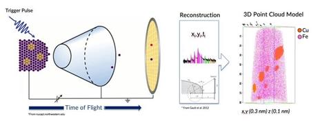
In an atom probe tomography experiment, we use the combination of a high electric field and a laser trigger pulse to take our specimen apart one atom at a time. In a process known as Reconstruction, we make a virtual model of the original sample. We use the flight time to determine the elemental species, the hit coordinate on a position-sensitive detector to determine the (x,y) position, and we get the z position through back-projection methods. The resulting image is a 3D dataset, where each voxel represents a spatially and isotopically resolved atom from the original specimen.
Atom probe tomography (APT) is a unique analytical tool capable of providing 3D atomic maps of any element in the periodic table with sub-nm spatial resolution and high analytical sensitivity (in the ppm range, in some cases). APT is currently employed by many of the largest semiconductor manufacturers in the world. It is used for process development, failure analysis, and competitive engineering to measure dopant profiles, composition, interfacial roughness, nucleation and clustering, diffusion, adhesion, and much more. However, the experimental techniques, data analysis routines, and commercial hardware that exist today often fail to provide the desired information, especially in the most advanced materials, on actual fabricated structures, and in fully integrated devices. For example, measurements of high-k dielectrics often obtain incorrect stoichiometry, and specimens frequently fracture during the experiment. In another example, it is very difficult to collect atom probe data on semiconductor/oxide and metal/oxide interfaces, which are important for optimizing transistors, interconnects, contacts, and integration schemes. Currently experiments must be optimized for one layer or the other, and specimens often fracture when traversing the interface, resulting in an incomplete measurement. In another example, fully integrated structures are often problematic due to the buried metal layers such as W and Ta, which due to their high evaporation field often lead to premature specimen fracture. To overcome this limitation, special simplified “test structures” are often fabricated with these or other problematic layers removed. These simplified test specimens are not necessarily representative of real-world structures.
Another issue that faces the industry is that the results of atom probe tomography measurements can be dependent on both the specimen geometry as well as how the data were collected. Finally, the sources of uncertainty, repeatability, and fracture during measurement are not well understood.
Improvements in APT instrument design would revolutionize atom probe tomography measurements for the semiconductor industry. Best practice guides and white papers would enable industry to make repeatable, faster, more accurate measurements with decreased uncertainty on currently available instruments. NIST data on optimal specimen geometry, data collection parameters, and analysis techniques would enable reliable materials measurement across the ecosystem. Reliable measurements on complex materials, structures, and devices at the atomic scale would enable industry to correlate process variations with performance in ways that are not currently possible.
Additional Technical Details
As part of the CHIPS Metrology Program, NIST has procured one of the first commercial deep ultraviolet atom probe microscopes. We will provide comparative analysis on specimens from industry collaborators and produce Best Practice Guides for optimizing measurements on this new commercial APT system. These guides will immediately improve the repeatability, reliability, and decrease uncertainty of APT experiments performed on currently available commercial instruments.
After five years we anticipate having determined optimal APT operation conditions for industry-relevant materials. In the meantime, the team is actively seeking opportunities for cooperative research with non-federal entities, particularly U.S. industry partners. Please contact the team for more information about partnership and collaboration opportunities.