
Official websites use .gov
A .gov website belongs to an official government organization in the United States.
Secure .gov websites use HTTPS
A lock (
) or https:// means you’ve safely connected to the .gov website. Share sensitive information only on official, secure websites.
Summary
To provide the necessary information for electronic material manufacturers to predict how and when failures will occur and enable lifetime analysis appropriate for their desired performance level through electrical, thermal and mechanical stress testing. The project focuses at present on 2D materials but develops core competencies that could be applied to a variety of electronic materials now and in the future.
Description
Manufacturing optimized devices that incorporate newly-emerging materials requires predictable performance throughout device lifetimes. Unexpected degradation in device performance, sometimes leading to failure, is often traceable to poor material reliability. Reliability is rooted in the stability of the atoms making up a material, and is determined by geometry, microstructure, chemistry, dimensional scale, proximity to other materials, and exposure to external stressors. Integration of powerful characterization techniques and reliability tests of materials under operational conditions improves fundamental understanding and accelerates development of highly-reliable materials and devices.
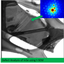
We develop relevant test approaches that can be readily adapted to the diverse, rapidly-moving environment of the 2D materials and microelectronics industry. We target the following:
- Techniques to measure atomic structure, crystallographic phase, grain structure, crystallographic texture, crystal defects, lattice strain, contaminants
- Imaging of 3D assemblies of 2D materials: moving toward characterization in real-life applications
- Time-resolved measurements of material performance and degradation under operational conditions
- Application of reliability physics concepts to predict material degradation
NIST has field emission scanning electron microscopes, focused ion beam microscopes, high resolution transmission electron microscopes, electrical testing systems, nanomaterial synthesis facilities, and spectroscopy instrumentation.
National Research Council Post-Doctoral Research Opportunities: (you will be leaving NIST website when selecting this link)
Nanometer-Scale Characterization and Reliability of 2D Materials
Transmission Scanning Electron Microscopy for Materials Characterization