
Official websites use .gov
A .gov website belongs to an official government organization in the United States.
Secure .gov websites use HTTPS
A lock (
) or https:// means you’ve safely connected to the .gov website. Share sensitive information only on official, secure websites.
Photonic Sensors
PHOTONIC CALORIMETER
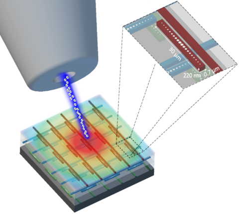
The Technology
By measuring the temperature rise in these silicon devices due to radiation absorption, NIST researchers have taken the first step toward a miniaturized version of the conventional “water calorimetry” technique — which determines radiation doses by measuring the heat that a beam of ionizing radiation produces in water. The chip-based device detects how heat energy affects the properties of light passing through microscopic channels on a chip being irradiated by gamma rays or an electron beam. By leveraging nanomanufacturing and telecommunications technology, the new sensor promises highly accurate readings at smaller dimensions than conventional sensor technology.
The chip is designed to contain an array of minuscule sensors in which light waves resonate at different frequencies depending on temperature. Each sensor is a couple of micrometers (millionths of a meter) in size, about 50 times smaller than the thickness of a human hair. The device is designed to measure the response to dose at the micrometer scale in materials and biological systems.
The NIST researchers use a laser to measure the frequencies at which light resonates on each sensor on the chip, which will enable them to build a map of temperature differences across a slice of the absorber. By stacking multiple chips, the technique could produce 3D images.
Advantages Over Existing Methods
The conventional approach for measuring radiation dose via calorimetry is designed for broad and uniform radiation beams, with widths on the order of 10 centimeters (4 inches), and is not suitable for the narrower, nonuniform beams used in many modern applications.
The chip-based device could realize absolute absorbed radiation dose at unprecedented spatial resolution 1,000 times better than current calorimetry technology.
Applications
Many current and emerging therapies use tightly focused, nonstandard radiation beams that can better target tumors with less chance of harming healthy tissue. Proton therapy beams, for example, may be only a few millimeters wide and deposit energy over areas so small that current detectors and methods are not able to provide measurements that are easily traceable to national standards.
Key Papers
Z. Ahmed et al. Assessing Radiation Hardness of Silicon Photonic Sensors. Scientific Reports. Aug. 29, 2018. DOI: 10.1038/s41598-018-31286-9
S. Bhandaru, S. Hu, D.M. Fleetwood and S.M. Weiss. Total Ionizing Dose Effects on Silicon Ring Resonators. IEEE Transactions on Nuclear Science. Jan. 28, 2015. DOI: 10.1109/TNS.2014.2387772
Q. Du et al. Real-time, in situ probing of gamma radiation damage with packaged integrated photonic chips. Photonics Research. Jan. 31, 2020. DOI: 10.1364/prj.379019
Key Patents
R. Tosh et al. Photonic calorimeter and process for performing calorimetry. United States Patent Application US 20190293809. Filed Feb. 15, 2019.
PHOTONIC DOSIMETER
The Technology
The photonic chips designed by NIST scientists are more radiation-resilient than traditional electronic chips, and thus work reliably in harsh environments. Because the chips are designed to be deployed in harsh environments, the NIST scientists exposed the devices to radiation doses 10,000 times higher than a typical medical therapy procedure. The sensors emerged undamaged, and their performance was unaffected.
The NIST scientists’ next objective is to incorporate radiation-sensitive materials into these photonic devices to create a sensor within an otherwise radiation-tolerant photonics platform. Unlike the photonic calorimeter, the photonic dosimeter incorporates materials that are known to change properties such as density and mechanical strain in response to radiation exposure, and it measures those.
In this way, scientists can be sure that the radiation-induced signal recorded by the device is due only to accurate sensing by the sensor element, without false signals due to radiation damage in other parts of the device itself.
Advantages Over Existing Methods
With micron-scale dimensions, photonic dosimeters would resolve dose and dose gradients at the scale of cells and bacteria, and enable dosimetry to be done at material boundaries or near surfaces where current methods fail. Moreover, their temperature response could be used as a separate, independent measure of dose for temperature compensation or self-calibration purposes, making them more versatile and deployable for a wider range of applications.
Applications
Measurements of radiation dose are increasingly needed in many kinds of harsh environments, including outer space for monitoring radiation damage to critical satellites. On Earth, there is a pressing need to measure, ideally in 3D, the dose delivered during the use of radiation in advanced manufacturing of nanometer-scale devices, sterilization of medical products, and the monitoring of high-radiation environments such as nuclear reactors.
Key Papers
G. Brunetti, I. McKenzie, F. Dell'Olio, M.N. Armenise and C. Ciminelli. Measured radiation effects on InGaAsP/InP ring resonators for space applications. Optics Express. Aug. 13, 2019. DOI: 10.1364/OE.27.024434
P. Casolaro et al. Real-time dosimetry with radiochromic films. Scientific Reports. March 29, 2019. DOI: 10.1038/s41598-019-41705-0
Key Patents
R. Tosh et al. Photonic dosimeter and process for performing dosimetry. United States Patent Application US 20190293808. Filed Feb. 15, 2019.
Contacts
-
(301) 975-5597
-
(301) 975-5591
-
(301) 975-5875
-
(301) 975-4121
-
(301) 975-5580
-
(301) 975-3517