
Official websites use .gov
A .gov website belongs to an official government organization in the United States.
Secure .gov websites use HTTPS
A lock (
) or https:// means you’ve safely connected to the .gov website. Share sensitive information only on official, secure websites.
Dimensional Metrology

The Technology
NIST researchers are developing a novel, quantum-accurate, chip-scale device that is designed to deliver dimensional measurements derived directly from the SI with comparable uncertainties to existing standards at substantially reduced cost and in less than one-thousandth the volume.
In the current industry standard method for length measurements, multiples of a known wavelength of light serve as a “ruler” for distance. Because the speed of light is a universal constant with a specific, defined value, if the frequency of the light is known exactly, so is the wavelength. The frequency of many optical transitions in atoms have been measured, resulting in a set of known wavelengths that can be used as length references, for example, in calibrating interferometers used for distance measurements.
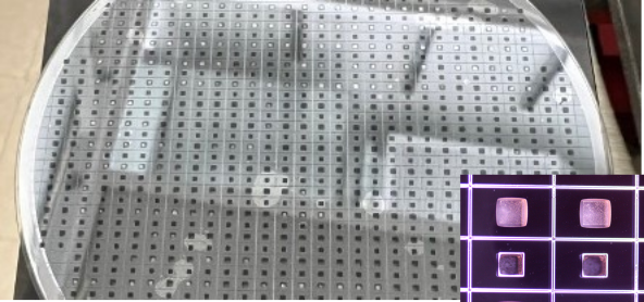
NIST’s chip-scale length standard now in development relies on the same principles in an unprecedentedly compact package. The atomic vapor is confined in a silicon-and-glass cell about 1 millimeter on a side. A tunable laser sweeps across a narrow range of frequencies to find the precise frequency at which an atomic transition takes place, and then locks the laser onto that frequency by a feedback system. The stabilized light is then routed using optical fibers to interferometers. Eventually, uncertainties are expected to be in the range of parts in 1011.
The researchers believe that the standards eventually could function with cells as small as one-thousandth of a cubic millimeter. They would be highly manufacturable, with hundreds of units on a single silicon wafer of the sort used in the microchip industry, thanks to existing microfabrication technology and rapidly expanding capabilities in the manufacture of photonic circuits.
Advantages Over Existing Methods
Existing commercial standards for length are based on a well-known wavelength of a helium-neon (He-Ne) laser. Such instruments are accurate to a few parts in a hundred million and typically cost around $10,000 per unit. They serve a broad range of industry sectors from aerospace to telecommunications.
But the instruments are unsuited to many uses because of their cost and size. (A typical He-Ne laser and its power unit take up about as much space as a laptop computer.) An inexpensive, chip-scale version of this wavelength standard could dramatically increase the range of potential uses in applications such as calibration of critical industrial instruments.
Applications
An instrument of such a scale could also be important for systems that transfer high-density, two-way information in light traveling through optical fibers. A process called wavelength-division multiplexing encodes a few or many dozens of multiple signals in simultaneous streams of different wavelengths. For that technique to work effectively, the wavelengths of the component streams must be carefully differentiated using a standard to avoid mixing.
Key Papers
Alexander Yulaev, Chad Ropp, John Kitching, Vladimir A. Aksyuk and Matthew T. Hummon. Chip-scale sub-Doppler atomic spectroscopy enabled by a metasurface integrated photonic emitter. Applied Physics Letters. Published Sept. 19, 2024. DOI: 10.1063/5.0222456
Yang Li, Donggyu B. Sohn, Matthew T. Hummon, Susan Schima and John Kitching. Wafer-scale fabrication of evacuated alkali vapor cells. Optics Letters. Published Aug. 28, 2024. DOI: 10.1364/OL.527351
M. T. Hummon et al. Photonic chip for laser stabilization to an atomic vapor with 10-11 instability. Optica. 2018. DOI: 10.1364/OPTICA.5.000443
J. Kitching et al. NIST on a Chip: Realizing SI units with microfabricated alkali vapour cells. Journal of Physics: Conference Series. June 1, 2016. DOI: 10.1088/1742-6596/723/1/012056
J. Kitching. Chip Scale Atomic Devices. Applied Physics Reviews. Aug. 14, 2018. DOI: 10.1063/1.5026238
Key Patents
J. Kitching. Alkali metal vapor cell apparatus and process for making alkali metal vapor cells. United States Patent Application US 2020/0002802. Jan. 2, 2020.
Contacts
-
(303) 497-4083